A metal base and a surface finish answer different questions.
浙江领潮电子科技有限公司 / Lingchao Electronics lists aluminum-base boards alongside nickel-plated, HASL and rosin-labelled PCB families. Its company description covers single-sided and double-sided circuit boards, drilling, imaging, lamination, plating and testing. The useful starting point is the construction and assembly process of your board—not a guessed layer count from a catalogue photograph.
The company traces its business to the Ruian Bethel circuit-board factory established in 1993. That predecessor history does not establish the incorporation date of today’s Zhejiang entity. The primary contact page locates the business in Pingyang’s Binhai New Area Electroplating Park, Building D09.
THERMAL CONSTRUCTION / RELEASE THE WHOLE STACK
Aluminum-base sourcing starts with the dielectric.
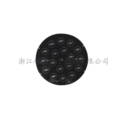
Aluminum-base PCB
Base family
Aluminum-base board
Published dimensions
No thickness, copper weight or thermal-dielectric grade stated
Release the metal thickness, alloy, copper weight and dielectric grade together. Ask for thermal conductivity with its test method and isolation withstand conditions, then match the board-to-heatsink interface and screw-hole drawing. Aluminum alone does not define the thermal or electrical performance.
Keep heat transfer and isolation in the same brief.
The official aluminum-base page supplies a family name and original board photograph. It gives no dielectric grade, thermal conductivity, isolation voltage, copper weight or construction thickness. Those values remain unspecified in the directory.
Thermal path: material grade and test method, expected dissipation and the board-to-heatsink interface.
Mechanical interface: alloy and thickness, mounting holes, outline, flatness, insulation around metal edges and assembly attachment.
Ask for one proposed construction against your drawing. Do not substitute an aluminum-base catalogue photo for a thermal model, or assume every exposed metal region is electrically isolated in the same way.
Three catalogue labels; three specifications to clarify.
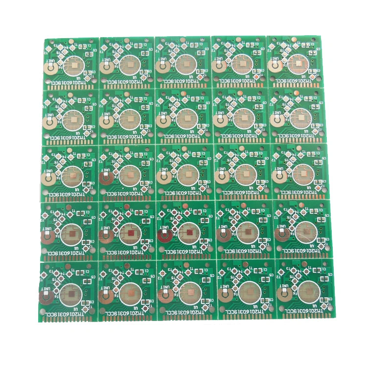
Nickel-plated PCB
Surface treatment
Nickel plating
Process definition
No nickel thickness, underplate or contact-life test stated
Identify the plated areas, nickel process and thickness, underlying copper and any additional finish. For a contact, release the mating material, force and wear test. For a solder joint, agree solderability after the planned storage interval. This title does not identify ENIG or hard gold.
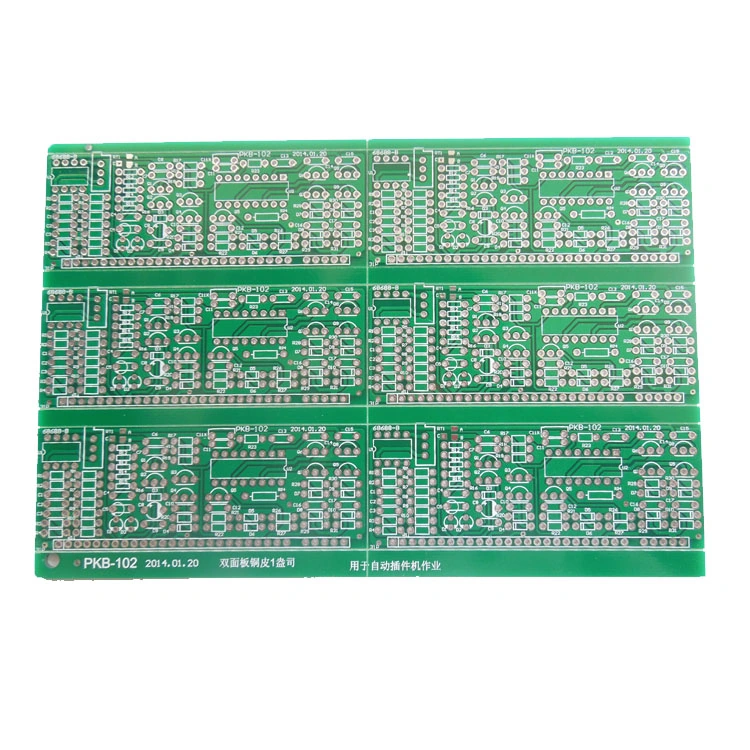
HASL PCB
Surface treatment
Hot-air solder levelling (喷锡)
Alloy definition
Leaded versus lead-free alloy not identified
State the solder alloy and lead-free requirement explicitly. Supply the assembly pitch, pad-flatness acceptance and thermal-exposure limits for the selected laminate. Agree storage, packaging and solderability inspection; a HASL photograph does not establish fine-pitch assembly compatibility.
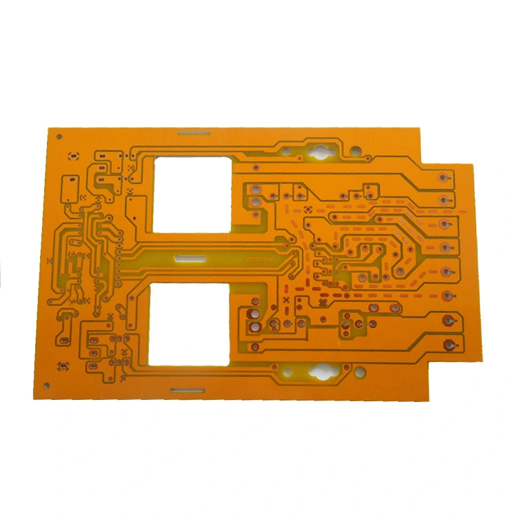
Rosin-labelled PCB
Manufacturer label
松香板 — rosin board
Coating definition
No chemistry, coating thickness or recognised finish designation stated
Ask what “rosin board” means for this quotation: the coating chemistry, application process, coverage and accepted specification. Agree cleaning, assembly conditions and post-storage solderability. Do not substitute this label for an OSP specification without the manufacturer’s explicit confirmation.
A finish title does not establish a complete stack.
“Nickel-plated” does not identify ENIG, an additional gold layer or a hard-gold contact system. “HASL” does not identify the alloy or promise lead-free processing. The rosin-board label does not identify an OSP chemistry or a recognised finish specification.
The source gives no layer count, trace/space limit or hole definition for these individual specimens. Those values cannot be recovered reliably by looking at pad shapes or board colour. Use the catalogue families to start a process discussion, then obtain the released construction and acceptance plan.
Ask which route will make and inspect your revision.
Drilling and panel geometry
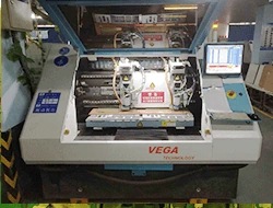
The homepage separately labels high-speed two-axis and six-axis drilling equipment; the corresponding photographs show workshop equipment. These labels do not supply drill size, registration accuracy or finished-hole limits. Release the drill table with plated/non-plated definitions and ask how hole and copper registration will be checked.
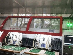
The outline-equipment entry is relevant to routed edges and slots. Provide the panel drawing, retention method, burr limits and dimensional inspection points, especially where a metal base must fit a heat sink.
Official two-axis drilling-equipment entry; no minimum hole or accuracy derived from the photograph.
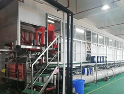
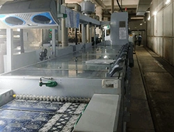
Official VCP automatic-plating entry. The same image is also used under a flying-probe label, so it is not used as photographic proof of flying-probe testing.
Plating and test coverage
The company describes automatic plating and copper-deposition processes. The homepage’s VCP-plating and flying-probe entries reuse the same line photograph. Keep that image-label mismatch separate from the company’s written testing statement; it does not demonstrate a photographed flying-probe machine.
For your order, request the released netlist, open/short coverage, acceptance criteria and report format. Define which plating or finish measurements accompany the lot. A production-line photograph cannot establish a finish thickness or confirm that every board receives a particular test.
Manufacturer-labelled outline-routing equipment; drawing-specific slot and edge tolerances require confirmation.Manufacturer-labelled HASL equipment; the photograph does not specify solder alloy or pad flatness.
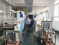
Etching and dimensional inspectionManufacturer-labelled automatic-etching line from the primary website.
Agree the copper weight, line geometry and measurement locations for the actual board. No numerical etching limit is published in the individual catalogue pages reviewed here. Ask for the proposed route, inspection sampling and lot documentation rather than combining unrelated equipment names into a capability guarantee.
SUPPLYING ENTITY / PINGYANG
Keep the contract, producing address and record scope aligned.
Primary company and contact information
The primary company website identifies Zhejiang Lingchao Electronic Technology Co., Ltd. (浙江领潮电子科技有限公司) and Building D09, Binhai New Area Electroplating Park, Pingyang, Wenzhou. Its contact-page telephone is 0577-63779666. The repeated product-page number “13800000000” is a placeholder and is not treated as a verified contact.
No mailbox-control test has been performed. Confirm the legal entity, producing location and authorised commercial contact on the quotation before transmitting controlled design data. A predecessor history or another branded domain does not replace that order-specific identity check.
Original public record
Wenzhou’s Science and Technology Bureau document 温市科管〔2017〕9号 lists the exact legal name in Pingyang, row 320 of the 2017 first-batch Zhejiang provincial technology-based SME list. It supports historical entity context; it is not a PCB quality certificate, current UL ownership check, inspection of a particular machine or approval of these product examples.
Current product qualification still depends on the required construction, supplying site and programme documents. No certification badge is added on the basis of that historical list.
DRAWING RELEASE / A USEFUL FIRST ENQUIRY
Send a construction brief, not just “aluminum” or “HASL”.
Reviewed 9 October 2026 against the primary company, contact and individual product pages, their corresponding original photographs and the original 2017 public record. Product parameters remain tied to the published family definition; unreported geometry and material grades are left unspecified.
SOURCE TRAIL
Sources behind this profile
Individual review dated 9 October 2026. The corresponding board and workshop images retain their actual source context. Nickel, HASL and rosin labels are not substituted with other finishes; the dated government record supports historical identity only.