

What this manufacturer makes
World Easy PCB manufactures double-sided and multilayer printed circuit boards in Huizhou. Its official profile describes a Hong Kong-owned business established in 1998, serving communications, computing, household appliances, industrial instrumentation and automotive electronics. The published range includes blind and buried vias and several surface-finish processes. The company overview provides an 18-layer ceiling and a 0.076 mm routing value. The listed 0.10 mm hole is not explicitly identified as a finished mechanical hole, so that filtering field remains unspecified.
Official company source reviewed- Manufacturing focus
- Double-sided and multilayer PCBs · Blind and buried vias · Industrial and communications boards
- Published footprint
- Guangdong
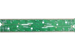
Multilayer PCB — up to 18 layers
Manufacturer reportedWorld Easy PCB lists multilayer PCB — up to 18 layers in its official manufacturing documentation. Board thickness: 0.2–4.0 mm. Line / space: 0.076 / 0.076 mm. Surface finishes listed: HASL, plated gold, OSP, immersion silver, tin and ENIG. Company overview capability. The 0.10 mm hole disclosure is not used as a finished mechanical-hole limit. Which stack-up, laminate grade, finished copper and acceptance criteria will be used for this board?
Company overview capability. The 0.10 mm hole disclosure is not used as a finished mechanical-hole limit.
- Layer count
- 2–18 layers
- Line / space
- 0.076 / 0.076 mm
- Finished hole
- —
- Impedance
- —
| Board thickness | 0.2–4.0 mm |
|---|---|
| Line / space | 0.076 / 0.076 mm |
| Surface finishes listed | HASL, plated gold, OSP, immersion silver, tin and ENIG |
| Technical source | wepcb.com · Manufacturer specification |
Published limits may refer to different constructions. Confirm the complete stack-up with the factory. A dash means no value was published.
Sources & review record.
Reviewed 2026-09-21. Manufacturer pages can change; confirm the current revision when requesting a quotation.
- World Easy PCB — product and technical documentationhttp://www.wepcb.com/about.html#capacitySource checked 2026-09-21Official website
- World Easy PCB — company informationhttp://www.wepcb.com/about.htmlSource checked 2026-09-21Official website
- World Easy PCB — company informationhttp://www.wepcb.com/Source checked 2026-09-21Official website
Make the first technical conversation useful.
Which stack-up, laminate grade, finished copper and acceptance criteria will be used for this board?
Attach the manufacturing brief
Layer stack-up, finished dimensions, copper weights, laminate grade, quantity and delivery destination.
Define acceptance
Finished-hole tolerance, impedance targets, coupon requirements, surface finish and permitted process substitutions.
Confirm the recipient
Agree the manufacturing legal entity, confidentiality terms and approved site before sharing production files.