

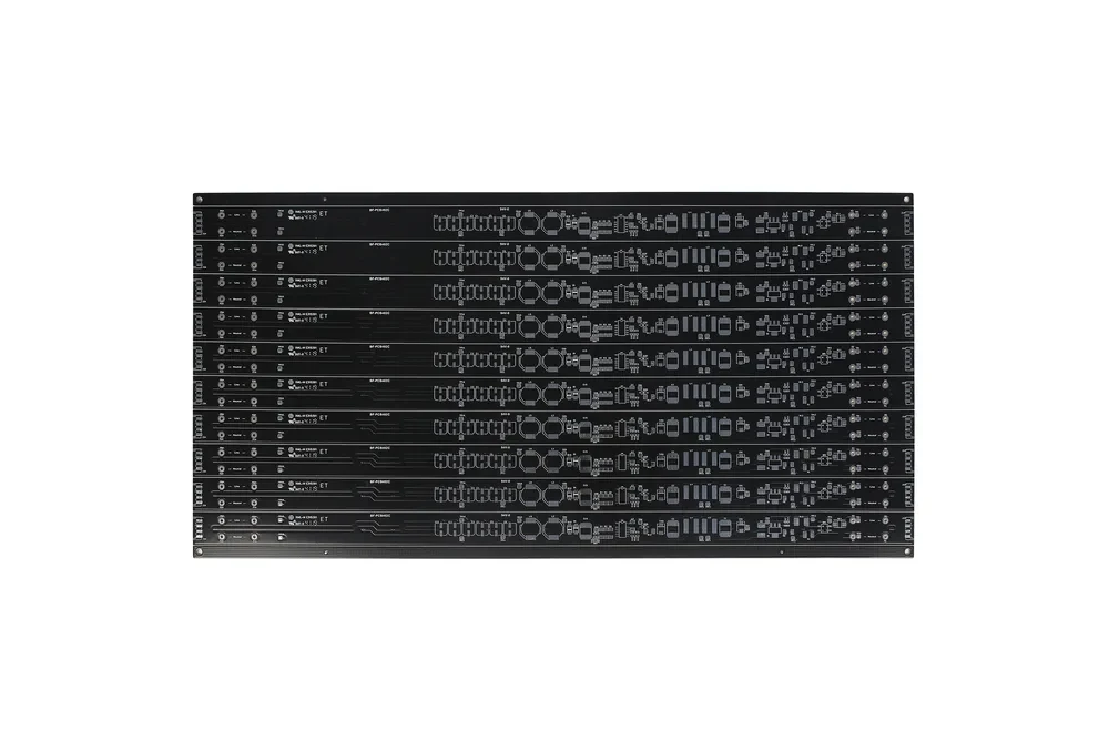
Four layers, six-ounce outer finished copper.
- Published material
- FR-4 Tg170; exact laminate grade not named
- Size / finished thickness
- 350.56 × 580 mm / 2.3 mm
- Copper distinction
- 6 oz outer finished; 6 oz inner base
- Line / space
- 14 / 14 mil
- Hole / wall copper
- 0.20 mm hole label; wall copper ≥25 μm
- Finish / mask
- HAL / gloss black
The catalogue describes communication use. For a power design, specify current, temperature-rise allowance, copper on every layer and thermal paths. “Six ounce” alone does not define a complete stack: the outer value is finished copper, while the inner value is base copper. Agree thickness measurements and acceptance locations in the order.
The dedicated heavy-copper routing table gives 6 oz base-copper line/space of 0.40/0.40 mm, whereas this product entry lists 14/14 mil (0.3556/0.3556 mm). Do not silently replace one with the other. Ask engineering which route supports the requested geometry and finished copper, including its etch allowance and inspection plan.
A two-layer RO4350B example with a 3 mm thickness label.
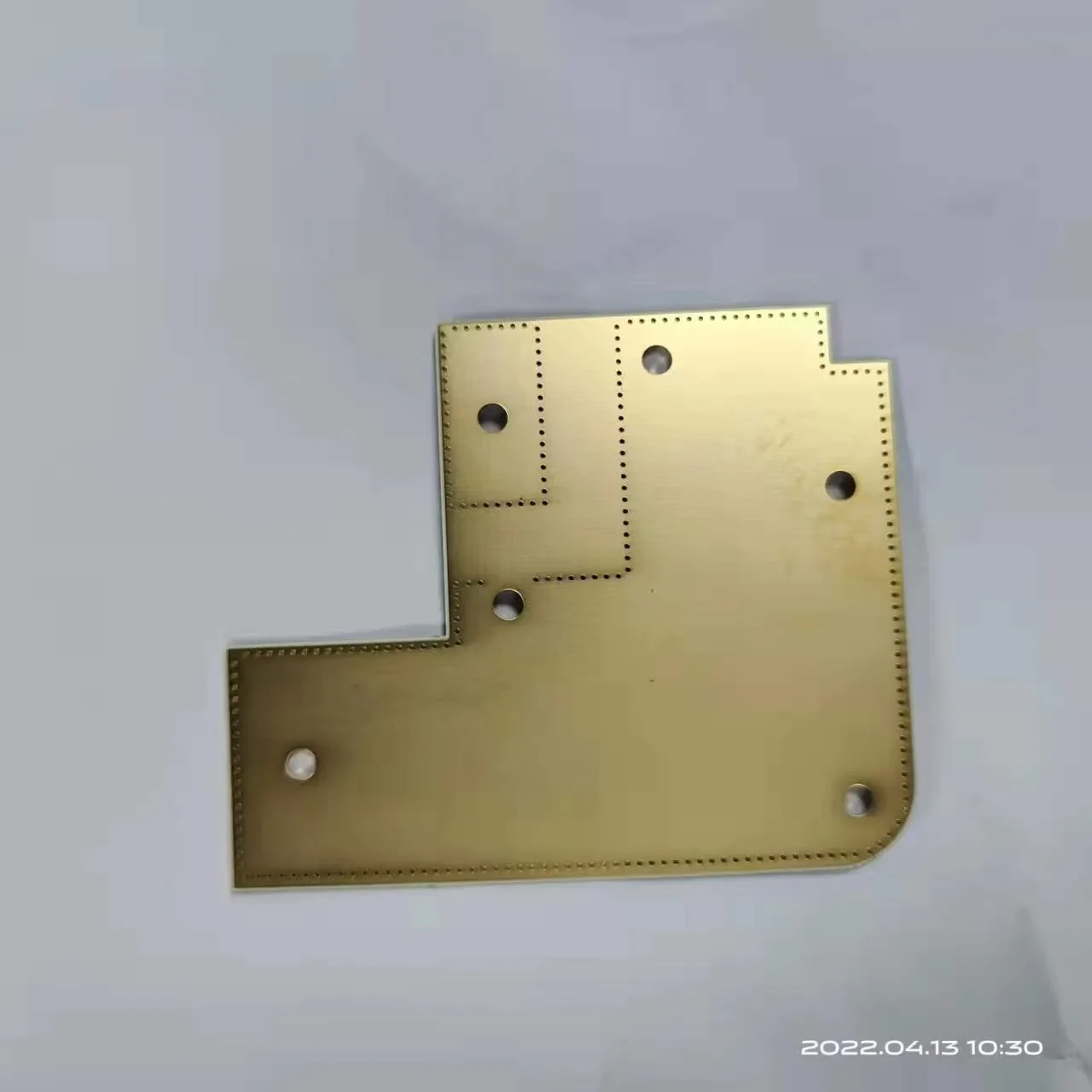
This individual entry names Rogers 4350B, two layers, 3 mm thickness, a 0.30 mm minimum-hole label and ENIG. It also describes an inner circuit exposed by slotting. The generic Rogers category table instead shows a different 1.6 mm, 89 ×105 mm, one-ounce construction. Those category values are not substituted into this product.
- Material
- RO4350B, as named in the entry
- Thickness
- 3 mm; thickness breakdown needs agreement
- Surface finish
- ENIG
- Minimum hole label
- 0.30 mm; finished definition not stated
- Routing / copper weight
- Not supplied for this individual entry
Send the RF stack, copper foil, dielectric thickness, operating band, controlled dimensions and any cavity or exposed-circuit detail. Ask whether 3 mm means laminate, finished board or the complete mechanical construction. A material name does not provide a loss measurement for the finished circuit.
Rogers’ own processing guide describes RO4350B as a glass-reinforced, ceramic-filled hydrocarbon-resin composite. We do not repeat the supplier category page’s claim that Rogers materials have no glass. Confirm the specific laminate and foil designation, sourcing traceability and permitted substitutions.
Four-layer via-in-pad, with ±10% impedance stated.
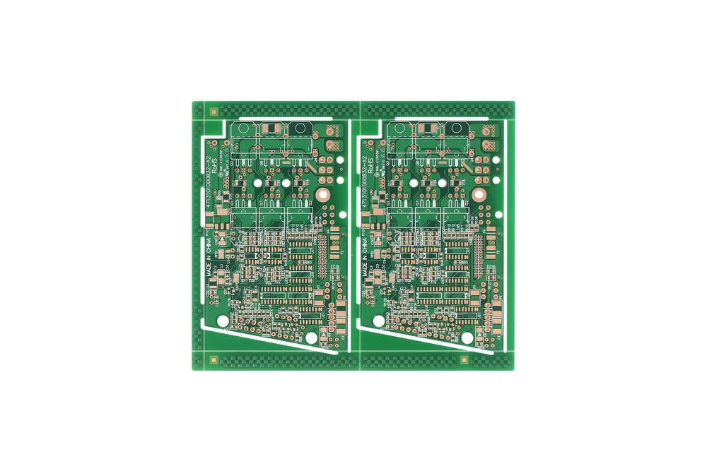
The entry lists FR-4 Tg180, 8/8 mil routing, a 0.25 mm minimum-hole label, 3 oz outer finished copper and immersion gold at 2 μin. Its stated impedance tolerance is ±10%. It does not supply the impedance target, reference layers or coupon geometry; include those in the RFQ.
Resolve these three drawing fields before release.
- Thickness: both the product and category pages print “1.6m”. We do not convert this to millimetres without confirmation.
- Inner copper: the product says 4 oz base copper; the category table says 3 oz. Confirm the actual copper-by-layer stack.
- Hole-wall copper: the row uses “1oz”, unlike the general table’s μm wall-thickness value. Request the required wall thickness and its measurement definition.
For via-in-pad assembly, define via filling, cap plating, dimple/flatness limits, pad geometry and reflow conditions. Ask for the test-coupon design and acceptance report; the image itself does not establish whether the vias are filled and capped.
Large outlines and inspected areas have different ceilings.
The general capability table lists a maximum board outline of 620 ×1200 mm, while its AOI inspection-area row gives 620 ×620 mm. For a long board, request the actual inspection coverage and handling plan; the outline maximum alone does not explain how the entire circuit is inspected.
Thickness follows layer count.
Published minimum board thickness is 0.20 mm at two layers, 0.35 mm at four, 0.65 mm at six, 1.0 mm at eight and 2.0 mm at sixteen. These are separate rows. The 0.20 mm minimum must not be carried into a sixteen-layer quotation.
Standard and advanced tolerances.
PTH diameter tolerance is ±0.075 mm Standard / ±0.05 mm Advanced. For 50–100 Ω controlled impedance, the table gives ±10% Standard / ±7% Advanced. Ask which route and report apply to the released construction.
The capability sheet names flying-probe or tooling electrical test, TDR and AOI. The equipment gallery does not label machine brands, models or quantities, so we do not infer an equipment inventory from photographs or file names. Agree electrical-test coverage, impedance coupons, microsection reporting and outgoing inspection. IPC Class 2 / Class 3 appears as an available design/test option, not an automatic qualification for every supplied board.
The lead-time table separates layer count, area and expedited service. Its fast column is one day at two layers, two days at four/six, three at eight and five at ten. These published estimates do not include a demonstrated start condition, material availability or your delivery destination. Request a committed engineering-release and shipment schedule.
Keep Shenzhen Victory distinct from similarly named suppliers.
The official footer names ShenZhen Victory Electronic Technology Co., Ltd. and an address at 101, Building 2, No. 7 Jianlong Jingfa Industrial Zone, Baoan Residents Council, Yuanshan Street, Longgang District, Shenzhen. This page concerns that Shenzhen business; it does not merge it with the separate Victory Giant group.
UL Product iQ’s primary E315391 entry names “SHENZHEN VICTORY ELECTRTONIC TECHNOLOGY CO LTD” as the listing holder, using that spelling, and identifies XML-4, XML-2(ASP1) and XML-M(ASP1) board models in category ZPMV2. This cross-checks a scoped listing, not every catalogue construction. Ask whether the ordered stack, laminate, thickness and marking fall within the applicable model and facility scope.
The website also claims ISO, IATF and other certifications, but this review has not established live issuer status for each of them. No additional certification badge is added. The current site’s staff numbers and time-in-business wording vary between sections, so they are not used as current audited metrics.
Official service email: sales@victorypcb.com. Confirm the legal entity on the quote, actual production site, approved outside processes and change-control requirements. Include the exact product brief in a PCBVerified RFQ rather than sending only a general layer count.
Compare RF manufacturing routes → · Prepare material-traceability questions →Sources behind this profile
Individually researched on 8 October 2026. Photos remain paired with their own entries. Conflicting units and copper rows are retained for clarification; generic process maxima are not substituted into the examples. UL and Rogers records cross-check specific claims, not the complete production performance of this factory.
- MANUFACTURER / IDENTITYCompany and Shenzhen address ↗
- MANUFACTURER / PROCESSManufacturing capability, test options and lead-time table ↗
- MANUFACTURER / HEAVY-COPPER EXAMPLEFour-layer six-ounce board and its original photo ↗
- MANUFACTURER / COPPER RULESCopper-dependent routing table ↗
- MANUFACTURER / RF EXAMPLETwo-layer Rogers 4350B product entry ↗
- MANUFACTURER / DIFFERENT RF CONSTRUCTIONRogers category table ↗
- MATERIAL MAKER / COMPOSITIONRogers RO4003C/RO4350B/RO4835 processing guide (PDF) ↗
- MANUFACTURER / VIA-IN-PAD EXAMPLEFour-layer board, parameters and original image ↗
- MANUFACTURER / CONFLICTING COPPER ROWImpedance category table ↗
- MANUFACTURER / QUALITYQuality systems and equipment gallery ↗
- UL / PRIMARY LISTINGE315391 holder and board model listing ↗