KUNSHAN SUXIN / CONSTRUCTION FIRST, PROCESS LIMITS SECOND
Eight actual board references, with a different acceptance brief for each.
Suxin’s catalogue spans double-sided boards, multilayers, flexible circuits and aluminium-base boards. The useful detail is in its individual titles: an 18-layer HDI board, a 10-layer HDI OSP board, a 6-layer chemical-gold board with gold fingers, a 2-layer FPC and a single-sided aluminium-base board. This page follows those constructions, their corresponding original pictures and the information an engineer needs to release them.
The company introduction says its single-sided, double-sided and multilayer production reaches 18 layers. Forty-six linked catalogue details were read separately for this review. Eight distinct references are selected below; repeated smartphone pictures and unnamed variations are not counted as different manufacturing qualifications.
HDI AND MULTILAYER / WRITE THE BUILDUP BEFORE USING THE LAYER COUNT
The 18-layer and 10-layer titles do not define the microvia architecture.
Corresponding manufacturer original shown whole. Numeric geometry is not inferred from the photograph.
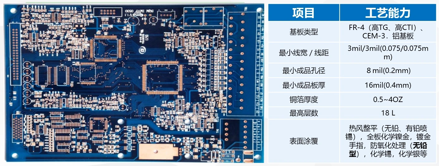
18-layer HDI catalogue reference
Catalogue identity
18L HDI板 identifies 18 layers and an HDI family. The adjoining multi-material process table is a general envelope, not the specification of this photograph.
Trace / space, finished hole, impedance
No design-specific values published
Engineering acceptance
Supply the buildup, via types, sequential lamination cycles, pad geometry, material grade and coupon plan. Ask for written acceptance of this combined stack; no laser drill, microvia reliability or 3 mil geometry is assigned from the title.
Corresponding manufacturer original shown whole. Numeric geometry is not inferred from the photograph.
10-layer HDI with OSP reference
Catalogue identity
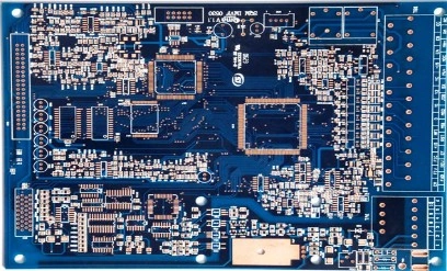
10L HDI OSP板 identifies 10 layers, HDI and OSP. Via architecture, coating supplier / thickness and geometry are not specified.
Trace / space, finished hole, impedance
No design-specific values published
Engineering acceptance
Agree the buildup and filled / capped via requirements, the OSP process, storage and assembly reflow limits, and the electrical and reliability records for the released revision.
Define the interconnect
Give the core / buildup sequence, blind and buried via locations, stacked versus staggered microvias, filled / capped requirements and lamination cycles. Ask which operations are performed at the producing site and which are subcontracted. The word HDI in a title supplies none of these design choices.
Define the reliability evidence
Agree the via acceptance, microsection location and method, copper requirement, thermal or reflow qualification and sampling for the actual released construction. A catalogue picture is not a reliability result, and an unlabelled production photograph does not establish a laser-drilling model or microvia process window.
A mechanically different ten-layer example
Corresponding manufacturer original shown whole. Numeric geometry is not inferred from the photograph.
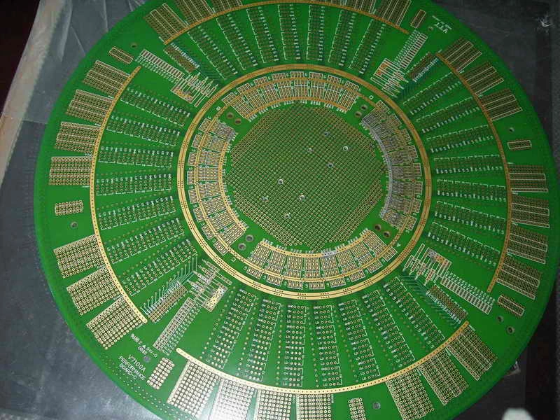
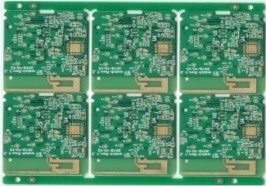
10-layer round-board reference
Catalogue identity
10L圆形板 names ten layers and a round outline. Diameter, thickness, routing tolerance, laminate and impedance are unreported.
Trace / space, finished hole, impedance
No design-specific values published
Engineering acceptance
Release a dimensioned outline with hole / slot datums, stack, finished thickness and electrical acceptance. Agree the panel / depanel route without scaling dimensions from this photograph.
The round-board title explicitly supplies ten layers, but its diameter, finished thickness, hole positions and routing tolerance are not provided. Send a dimensioned drawing and specify the mechanical datums and panel / depanel method. A round outline is not evidence of RF performance; no frequency band or controlled-impedance tolerance is attached to this reference.
THE MATRIX BESIDE THE 18-LAYER PHOTOGRAPH / ONE GENERAL ENVELOPE
Read the material list and process minima without turning them into one promised stack.
The original 18-layer HDI image contains a table headed “Project / Process capability.” It lists FR-4 with high Tg / high CTI, CEM-3 and aluminium base together. That breadth matters: the table describes the manufacturer’s general process range, rather than identifying the laminate and every limit of the blue photographed board.
Materials
FR-4 (high Tg, high CTI), CEM-3 and aluminium base. No approved brand, grade, Tg number or CTI value is given.
Trace / space
3 mil / 3 mil, also printed as 0.075 / 0.075 mm. The source’s rounded units are retained; ask which drawing acceptance units govern.
Finished hole
8 mil (0.2 mm), explicitly described as minimum finished hole. Plating requirement, tolerance and suitable stack are not specified.
Thickness and copper
Minimum finished board thickness 16 mil (0.4 mm); copper 0.5–4 oz. The table does not identify base versus finished copper or a layer-by-layer stack.
Maximum layers
18 L. This does not mean an 18-layer aluminium-base board, an 18-layer CEM-3 construction or a 0.4 mm 18-layer board is accepted.
Finish choices
Leaded / lead-free hot-air levelling, full-board chemical nickel-gold, plated gold fingers, lead-free anti-oxidation, chemical tin and chemical silver. A choice list is not one combined finish.
No impedance tolerance appears in the matrix. The eight product records therefore use the layer count stated by their own title and leave design-specific trace, spacing, hole and impedance values unknown. Send the intended stack, copper, finished hole and geometry together for written engineering acceptance.
CHEMICAL-GOLD PADS AND GOLD FINGERS / TWO DIFFERENT SURFACES
Specify solderability on the pads and contact life at the connector.
Corresponding manufacturer original shown whole. Numeric geometry is not inferred from the photograph.
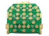
6-layer chemical-gold and gold-finger reference
Catalogue identity
6L化金+金手指 names six layers, chemical-gold pads and gold fingers. Contact gold type, hardness, thickness and bevel are not specified.
Trace / space, finished hole, impedance
No design-specific values published
Engineering acceptance
Define solder-pad finish separately from the mating contacts: deposit thickness, required hardness, mating cycles, connector card thickness and bevel geometry.
01 / PAD FINISH
Identify the required chemical nickel-gold process, deposits and applicable acceptance specification. “Chemical gold” alone does not supply a named ENIG specification or measured thickness.
02 / MATING CONTACT
State contact gold type, hardness, deposit thickness and mating cycles separately. The gold-finger title does not establish hard-gold plating, wear life or the nickel barrier.
03 / MECHANICAL FIT
Release card thickness, pad dimensions, edge setback and bevel. Confirm the connector interface and how it will be inspected before comparing the quote.
Two simpler chemical-gold references
Corresponding manufacturer original shown whole. Numeric geometry is not inferred from the photograph.
2-layer chemical-gold board
Catalogue identity
2L化金板 identifies two layers and chemical-gold finish. Exact substrate grade, nickel / gold deposits and acceptance specification are not given.
Trace / space, finished hole, impedance
No design-specific values published
Engineering acceptance
State the laminate, stack, finished thickness, copper and required deposit / solderability acceptance. Ask Suxin to confirm the named finish process and your assembly conditions.
Corresponding manufacturer original shown whole. Numeric geometry is not inferred from the photograph.
4-layer chemical-gold board reference
Catalogue identity
4L化金板 names four layers and chemical gold. The small original photograph is preserved rather than enlarged into a fabricated engineering drawing.
Trace / space, finished hole, impedance
No design-specific values published
Engineering acceptance
Specify the four-layer stack and material, finished copper / thickness, surface-finish deposits and any impedance / coupon requirement. Confirm those values for this design, not from the general sheet.
The two- and four-layer titles identify layer count and finish family. Neither provides a stackup or material grade. Likewise, the 10-layer HDI OSP reference needs the OSP supplier / process, storage condition and allowed assembly profile agreed for the order; an OSP label is not a guaranteed reflow-cycle count.
TWO-LAYER FPC / THE DRAWING MUST DESCRIBE HOW IT BENDS
Distinguish a one-time installation fold from a moving flex connection.
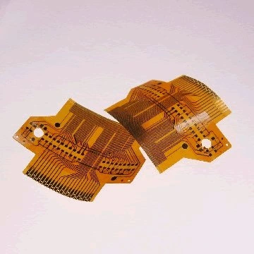
Corresponding manufacturer original shown whole. Numeric geometry is not inferred from the photograph.
2-layer flexible-circuit reference
Catalogue identity
2L FPC names two layers. Polyimide grade, adhesive system, coverlay, stiffeners and dynamic bend rating are not published.
Trace / space, finished hole, impedance
No design-specific values published
Engineering acceptance
Provide the flex stack, bend-zone and connector drawings, bend radius and cycle count, copper type, coverlay registration and stiffener / adhesive requirements.
Route and material
Identify the bend zone, bend direction, radius and cycle requirement. Specify base film, adhesive or adhesiveless construction, copper type and thickness, coverlay openings and any plating in the flexing region. The original title does not give a dynamic flex rating or permit an inferred minimum radius.
Termination and assembly
Dimension the connector tail and stiffeners, adhesive thickness, registration and finished contact thickness. Identify component / solder areas and the assembly process. The visible shape does not establish rigid-flex construction, populated assembly service or a connector manufacturer’s fit qualification.
The flex category contains several other unnamed geometries. These demonstrate catalogue variety, but repeating their pictures would not answer the engineering questions above. Use the explicitly named 2-layer FPC as the starting reference and ask for acceptance of the actual moving or static application.
SINGLE-SIDED ALUMINIUM BASE / INSULATION IS PART OF THE THERMAL SPECIFICATION
Agree the dielectric and mechanical interface, not just the base metal.
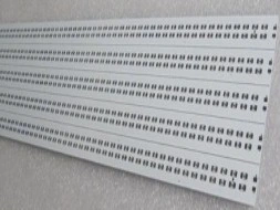
Corresponding manufacturer original shown whole. Numeric geometry is not inferred from the photograph.
Single-layer aluminium-base reference
Catalogue identity
单面铝基板 identifies single-sided circuitry and aluminium base. Dielectric grade, thermal conductivity, base alloy and dimensions are not supplied.
Trace / space, finished hole, impedance
No design-specific values published
Engineering acceptance
Define circuit copper, dielectric thickness and thermal test method, isolation acceptance, base alloy and thickness, flatness, mounting holes and housing interface. Clarify bare-board scope.
Circuit to base
Specify copper, dielectric thickness and grade, thermal-property test method, working voltage and insulation acceptance. The official title identifies aluminium base, but provides no conductivity, breakdown voltage, alloy or layer-by-layer thermal resistance.
Base to housing
Define base thickness, flatness, deburring, holes / slots and the interface surface. Agree the mounting and thermal-interface arrangement. Other catalogue photographs show LED components on some boards; that is not a reviewed statement that Suxin supplies populated LED assemblies or a qualified luminaire.
The general sheet’s 18-layer maximum and 3 mil geometry are not assigned to this single-sided metal-base reference. Request the accepted dielectric / copper / outline combination and the relevant inspection report for the exact board.
OFFICIAL PRODUCTION GALLERY / ASK FOR THE ROUTE BEHIND THE PICTURE
Use the workshop photographs to request an identifiable process and test record.
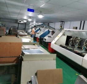
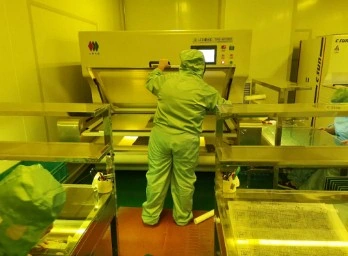
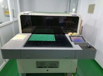
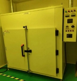
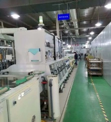
Original production-gallery machine-area photograph. The website does not provide a typed model, quantity or inspection date.Original yellow-lit production-area photograph. No LDI or laser-drilling specification is assigned from its appearance.Original production-gallery line photograph. Current installed capacity and the order’s routing remain to be confirmed.Original production-gallery instrument photograph. It does not provide a configured test method or a calibrated order result.Original production-gallery cabinet photograph. The website supplies no typed operating specification.Original production-gallery workshop photograph. A displayed machine is not a commitment to an available production slot.
The production page publishes photographs without an accompanying typed equipment register. The company’s undated advantage image mentions 25 high-end machines and 200+ employees, but gives no date, asset identification or currently available capacity. The buyer’s useful next step is a route sheet for the released revision: imaging, drilling, lamination, plating, finish, outline and inspection, with the producing site and any external operations identified.
For HDI, request the actual microvia and lamination route. For flex, request the coverlay / stiffener process. For aluminium base, request the dielectric and insulation route. Agree artwork / netlist revision, optical inspection, continuity / isolation and any impedance, microsection or application-specific tests as separate shipment records.
MANUFACTURER-HOSTED COPIES / HOLDER, DATE AND CONSTRUCTION MATTER
A single-layer UL inspection is not an 18-layer HDI approval.
UL E324216: historical file and inspection copies
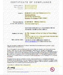
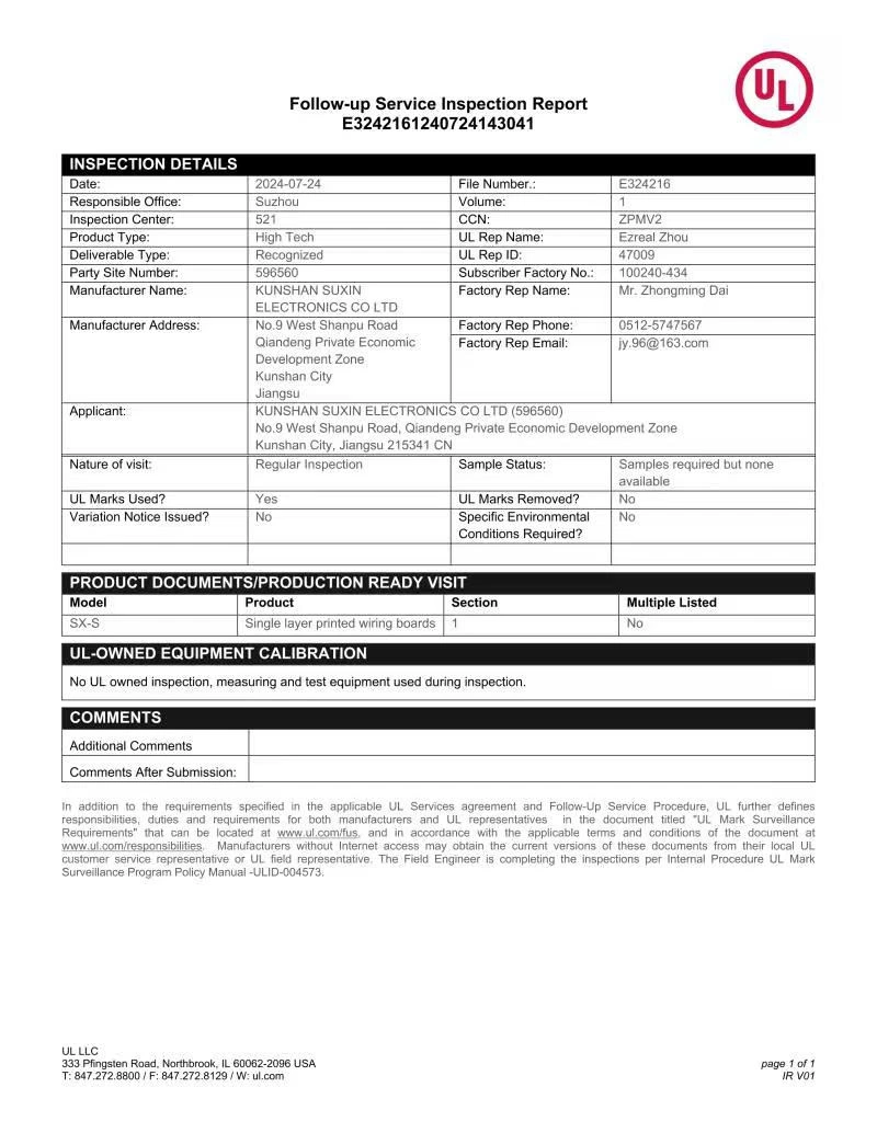
The 17 August 2012 certificate copy names KUNSHAN SUXIN ELECTRONICS CO LTD and file E324216. The 24 July 2024 follow-up inspection report also names that holder and No. 9 West Shanpu Road, and specifically identifies SX-S single-layer printed wiring boards, section 1, CCN ZPMV2. It says samples were required but none were available.
These are manufacturer-hosted historical records. The reviewed sources do not include a current Product iQ listing or a construction annex for the HDI, flex or aluminium references. Match the ordered construction and producing site to the current record rather than extending SX-S to the whole catalogue.
View the original 2012 UL certificate copyManufacturer-hosted UL certificate copy, dated 17 August 2012, file E324216. Not a current database verification.View the original 2024 follow-up reportManufacturer-hosted follow-up inspection report of 24 July 2024: SX-S single-layer printed wiring boards.
Management-system dates need a fresh check
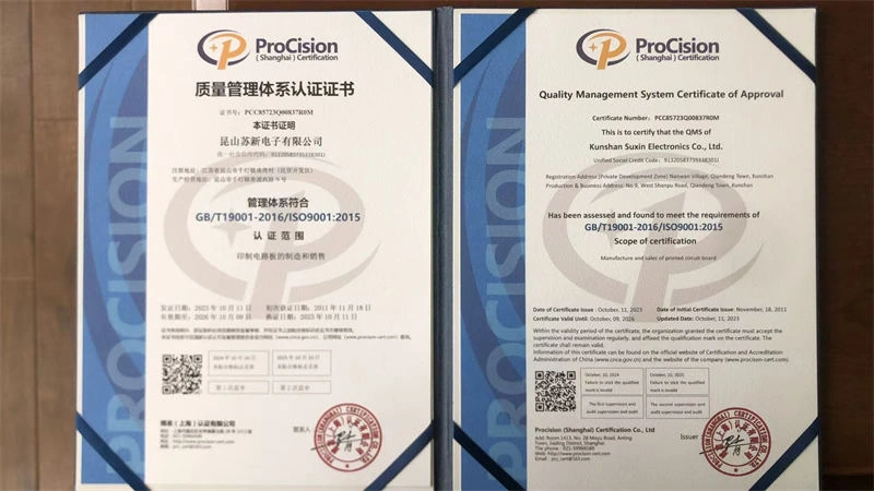
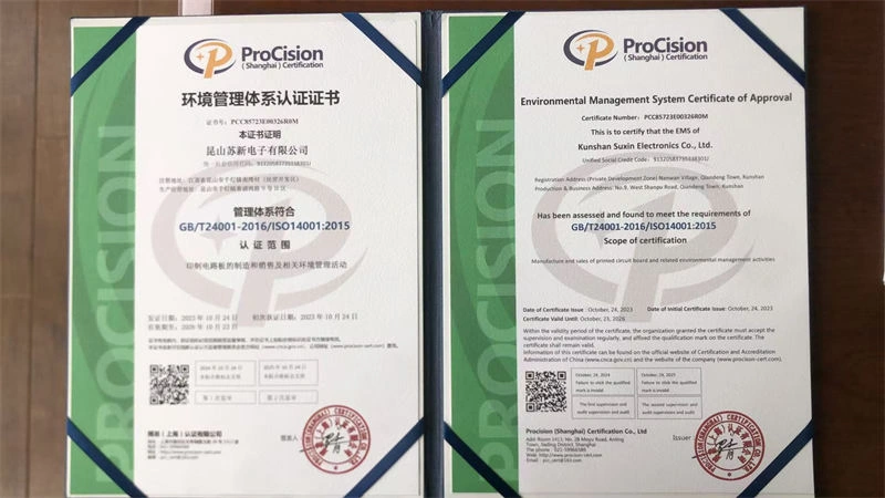
The ProCision ISO 9001 copy PCCS723Q008370R0M runs from 11 October 2023 to 9 October 2026, the date of this review. Request the renewal and issuer status before relying on it for a new order. The ISO 14001 copy PCCS723E003268R0M runs from 24 October 2023 to 23 October 2026.
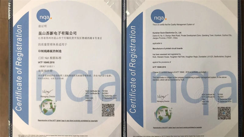
The NQA IATF copy NQAT87956 ended 21 September 2024 and excludes product design. These copies do not establish current automotive qualification, a customer-specific approval or the quality of a particular board.
View the ISO 9001 copy and expiry dateManufacturer-hosted ISO 9001 copy ending 9 October 2026. Current renewal and issuer status require confirmation.View the ISO 14001 copy and scopeManufacturer-hosted ISO 14001 copy ending 23 October 2026; manufacture and sale of printed circuit boards.View the historical IATF copyManufacturer-hosted IATF copy ending 21 September 2024. Product design is excluded.
Older high-tech, safety and other certificate pictures are also present, including a 2018 three-year high-tech copy and a safety classification ending December 2023. They are not converted into current certification badges. Application-sector lists in the introduction are not aerospace, medical or military product approvals.
QIANDENG, KUNSHAN / LEGAL NAME, PRODUCTION ADDRESS AND DATED GOVERNMENT RECORD
Confirm the same entity will contract, fabricate and release the lot.
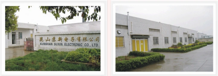
Official company-site factory photographs. They are original manufacturer disclosures, not a current site visit.
The about and contact pages name 昆山苏新电子有限公司. The contact page gives Area B, No. 9 West Shanpu Road, Qiandeng, Kunshan, Jiangsu, 0512-57475672 / 139-0626-3725 and jy.96@163.com, with Mr. Zhang as contact.
The footer uses the variant 昆山苏新电子科技有限公司. Do not assume this is a legal rename or a second qualified producing entity. Confirm the purchase-order, invoice and production identities from current documents. The generic header telephone and the placeholder hotline on some product pages are excluded; the contact-page mailbox has not been control-tested.
Kunshan clean-production assessment: a specific, dated result
The Kunshan government original notice posted 15 April 2025, with a document date of 19 November 2024, lists 昆山苏新电子有限公司, Qiandeng, row 83 among 108 enterprises that passed clean-production audit assessment. It refers to assessments in June–October 2024 and requires further implementation and acceptance-report work.
This supports the exact company-name / locality match and that assessment result. It is not final acceptance, a PCB quality certification or an independent audit by PCBVerified.
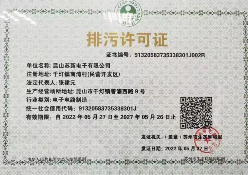
The manufacturer-hosted discharge-permit copy names the same company, unified credit code 91320583735338301J, permit 91320583735338301J002R, electronic-circuit manufacturing and production at No. 9 West Shanpu Road. Its printed period is 27 May 2022–26 May 2027. The registered address is separately written as Nanwan Village, Qiandeng, private development zone. A live government permit-status query was not reviewed.
Read the manufacturer-hosted permit copyManufacturer-hosted discharge-permit copy: printed validity 27 May 2022–26 May 2027. Not a live regulatory status check.
RELEASE PACKAGE / ONE ENGINEERING RESPONSE FOR THE ACTUAL CONSTRUCTION
Ask Suxin to accept the combined design, finish and inspection requirements.
Identify the route. HDI buildup, conventional multilayer, gold-finger contact, static / dynamic FPC or single-sided aluminium base, with the selected catalogue reference as context.
Release the drawing. Stack, exact material grade, finished thickness, copper, trace / space, finished holes, outline and any impedance requirement. Do not substitute the general matrix for this combined acceptance.
Resolve the interface. Via architecture, solder-pad versus mating-contact finish, flex bend / stiffener / tail, or dielectric and housing interface.
Agree the manufacturing and evidence scope. Producing site, external steps, artwork and netlist reference, lot trace, optical / electrical inspection and application-specific reports.
Refresh required qualification records. Current issuer status, construction scope and renewal dates, especially the ISO 9001 copy ending on the review date and the historical IATF / UL records.
Reviewed 9 October 2026. Eight independently mapped catalogue references are selectable here, on the existing Suxin factory URL. The catalogue’s 0.00 price fields are placeholders and are not presented as quotations.
Company identity, four catalogue families, 46 linked detail pages, corresponding original images and the Kunshan government original were reviewed separately. Unnamed duplicates, customer-logo decorations, placeholder prices and telephone fields are not qualifications or product specifications.