

A group capability is not a site assignment.
Shennan Circuits Co., Ltd. (深南电路股份有限公司, SCC) was founded in 1984 and is headquartered in Shenzhen. Its official introduction identifies manufacturing facilities in Shenzhen, Wuxi and Nantong. Its 2026 half-year exchange filing confirms the legal name and the three principal business lines; the filing does not assign this PCB process table to a particular factory.
The contact directory separately lists the Longgang headquarters at 1639 Yanlong Avenue, the Nanshan address at 99 Qiaocheng East Road, Wuxi at 18 Changjiang East Road and Nantong at 168 Hope Avenue. Ask which manufacturing operation and contracting entity will own fabrication, changes and final acceptance. The general contact mailbox is not evidence that every site can make the same stack-up.
Production repeatability and sample capability are separate questions.
The reviewed English PCB page separates “Mass” from “Sample”. Values below retain that separation. They are individual process-table entries, not a promise that the smallest drill, highest layer count, thickest copper and largest outline can be combined.
| Process item | Mass column | Sample column |
|---|---|---|
| Layers | 2–68 | 120 |
| Maximum thickness | 10 mm | 14 mm |
| Outer line / space | 2.5 / 2.5 mil | 2.2 / 2.2 mil |
| Maximum copper | 6 oz | 30 oz |
| Mechanical drill diameter | ≥0.15 mm | ≥0.10 mm |
| Backplane finished size | 1,250 × 570 mm | 1,320 × 600 mm |
Do not turn a drill-tool value into a finished aperture.
The table labels the mechanical row as drill diameter. A hole in your drawing needs a finished size, tolerance, plating requirement and, where relevant, a connector fit. The company's directory filter therefore leaves finished-hole capability unspecified rather than copying the mechanical-drill value.
Three boards, three engineering discussions.
These named examples are displayed on the same official PCB page. The individual entries give useful construction data but no product revision date or guarantee of current production availability. Ask for the corresponding current drawing and manufacturing route before using them as a quotation basis.
A 68-layer board where hole definition matters
The catalogue gives a 9.5 mm board with a 0.46 mm finished hole and a 20.7:1 aspect ratio. Here, unlike the generic drill row, the aperture is explicitly labelled finished.
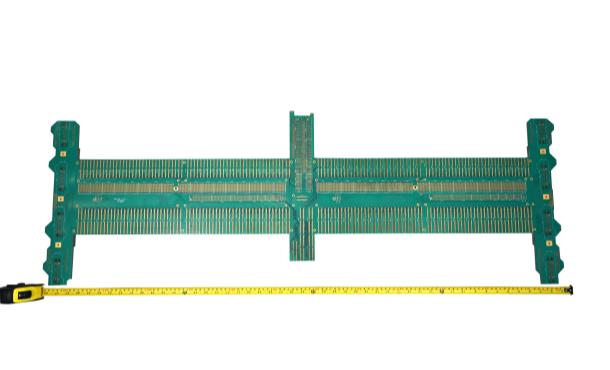
- Layers / thickness
- 68 / 9.5 mm
- Catalogue panel size
- 1,370 × 530 mm
- Finished hole
- 0.46 mm
- Aspect ratio
- 20.7:1
- Material, source wording
- Nelco N4000-13EP SI
Resolve the size scope: this example calls 1,370 × 530 mm a panel size, while the generic table lists different finished-board dimensions. Request the actual outline, panel drawing, connector-hole fit and proposed press-fit qualification; do not replace one definition with the other.
Hybrid material and thermal interfaces
The catalogue names a metal-based power-amplifier construction with Rogers4350B and FR-4. Its 1 oz entry describes copper thickness; it does not define the copper-base geometry, heat flow or an order-specific laminate stack-up.
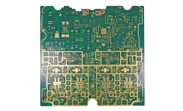
- Layers
- 12
- Thickness
- 2.6 mm
- Copper, catalogue entry
- 1 oz
- Material description
- Rogers4350B + FR-4
- Application
- Base-station power amplifier
Ask for: the RF-layer positions, copper-base and dielectric cross-section, heat-transfer assumptions and applicable flatness test. A material name alone does not establish loss, bond reliability or thermal resistance.
A ten-layer RF hybrid needs its own acceptance plan
The ODU example gives RO4350 plus FR-4, ten layers and a 2.0 mm thickness. It supplies no insertion-loss limit or controlled-impedance tolerance. Those values belong in the project's electrical acceptance requirements.
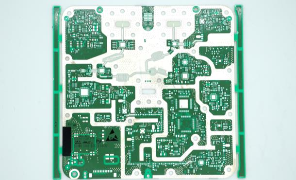
- Layers / thickness
- 10 / 2.0 mm
- Copper
- 1 oz
- Material, source wording
- RO4350 + FR-4
- Application
- Microwave
Send with the RFQ: the RF frequency range, dielectric thicknesses, copper roughness requirement, surface finish and agreed coupon/test method. Confirm the exact laminate grade rather than extending the shorthand “RO4350” to an unlisted substitute.
Make the engineering reply comparable.
- Name the intended stageIdentify prototype, qualification lot or repeat production. Ask which entries in the Mass / Sample table govern the proposed route.
- Name the construction and factoryAttach stack-up, copper by layer, material grade, finished outline and hole table. Request a named manufacturing site and a list of any external process steps.
- Name the evidence at deliveryAgree electrical test, coupon results, cross-sections, dimensional checks and traceability. For assembly, add BOM, placement and a separate functional-test plan.
Sources behind this profile
Reviewed on 8 October 2026. Product and process statements come from the official PCB page; the exchange filing cross-checks the corporate identity and business lines. No independent factory audit, material procurement verification or certification badge is implied.
- MANUFACTURER / COMPANYSCC introduction and manufacturing footprint ↗
- MANUFACTURER / PROCESS & EXAMPLESPCB page: Mass / Sample table and named product entries ↗
- MANUFACTURER / LOCATIONSSeparate headquarters, Nanshan, Wuxi and Nantong contacts ↗
- EXCHANGE FILING / ENTITY2026 half-year report: company name and principal businesses, printed pages 7 and 10 ↗