Power path
Release copper distribution, conductor geometry and plated connections together.


MANUFACTURER DOSSIER
湖南维胜科技电路板有限公司 · Hunan
This directory record is for 湖南维胜科技电路板有限公司, associated with the MFS Technology (PCB) operation in Changsha. The MFS website separately lists MFS Technology (Hunan) and MFS Technology (PCB) at 10 Dong Er Road, with different telephone numbers. Its PCB tab dates that operation to 1991 and describes heavy-copper boards for power-management and planar-transformer applications.
That distinction matters when an order spans a rigid power board, a flex interconnect and component assembly. Agree the contracting entity, fabrication site and assembly responsibilities with the quotation. A shared group website or street address does not make every process and certificate interchangeable.
The group catalogue below is useful for discussing a construction. The PCB-operation tab supplies the site association; the quoted limits retain their separate catalogue conditions. For the group's flex-focused Changsha profile, see MFS Technology (Hunan).

Release copper distribution, conductor geometry and plated connections together.
Define coin contact, flatness and the assembled thermal interface.
Separate the rigid-region stack from the flex zone and its bend duty.
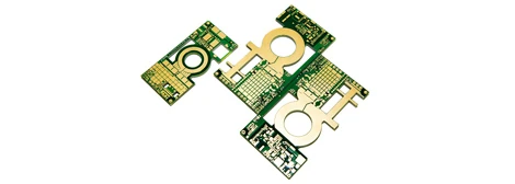
The catalogue places these statements beside this rigid-board image. It does not identify which layers carry 10 oz copper or whether the figure is starting foil or finished copper.
Provide the copper schedule by layer, pad and thermal-clearance rules, via map and the current path. Ask the factory to review etching, resin fill, lamination and hole-wall requirements on that exact stack. A copper-weight headline does not replace an agreed temperature-rise requirement or connection test.
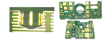
This adjacent entry has a different set of statements. Do not combine its 32-layer ceiling and impedance figure with the first entry's copper construction without a feasibility review.
Show the depth reference, cavity or recess boundary, remaining material and inspection datum. Where an impedance-controlled region shares the stack with heavy copper, define its dielectric geometry and coupon acceptance. Request the proposed stack and a marked-up drawing so the electrical and mechanical features have the same revision.
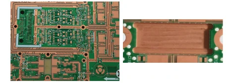
The product panel states Embedded I Coin, ENIG finishing and coin inner flatness control <30 µm. That is the source's stated flatness characteristic; it is not an overall board-bow limit, surface-height tolerance or measured thermal resistance.
Define the coin section, its location and the surface contacted by the component or heat spreader. Agree the flatness measurement datum and method, finish thickness, insulation boundary and attachment. Show the thermal interface material and mechanical load in the assembled design. Ask which inspection record will accompany the first lot.
MFS also describes 2.5D cavities and thermal simulation at group level. If a recessed component is part of your design, give the cavity floor and clearance drawing; agree the remaining dielectric and electrical test independently of the coin feature.
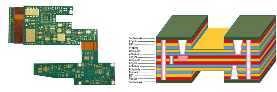
The group product page lists 1–12 layers and 0.20–2.4 mm board thickness, blind/buried vias, controlled-depth drilling/routing, blind-via fill and edge plating. It names static and multiple-bend applications. Those ranges describe a family; they do not state the flex-zone thickness, bend radius or qualified cycle life of one board.
Identify the rigid and flexible region layer counts separately. Release the copper type, coverlay openings, transition support, unbonded zones and any stiffeners. State whether the flex is installed once or repeatedly moves, with its bend radius, motion and test duty.
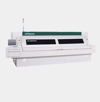
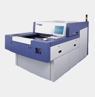
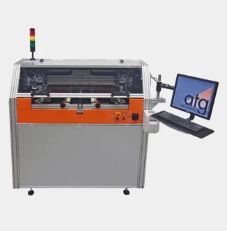
The group facilities catalogue also names laser drills, copper plating, AOI/AVI, X-ray inspection, thermal-shock and hi-pot equipment. It does not allocate every machine to this Changsha PCB entity. Ask the proposed plant to confirm the equipment and current inspection methods assigned to your order.
Approve the layer/copper schedule, finished-hole definitions, depth drawing, materials and any coin or flex interface. Resolve departures in a marked-up DFM response.
Agree the sectioning, coin/connection geometry and electrical tests. Define which measurements are lot records and which are development qualification.
Tie material identity, approved revisions, test results and assembly scope to the delivered lot. Keep site or material changes under written approval for repeats.
The capability page separates prototype and mass-production turnaround figures: double-sided PCB 6/14 days and multilayer PCB 8/18 days. Treat them as catalogue estimates; confirm the actual start conditions, material availability, outsourced steps and shipment date on the quotation.
The manufacturer-hosted TÜV Rheinland IATF copy names MFS Technology (PCB) Co., Ltd. at No. 10 Donger Road, Changsha, and IATF number 0533309. It prints 25 July 2024–24 July 2027 and covers PCB manufacture, excluding product design.
The ISO 9001 copy prints unified social credit code 91430100616600709F, the same registration/operation address and PCB manufacturing scope, with 24 August 2024–23 August 2027 validity. These are readable hosted copies; their current issuer status has not been independently checked here. Do not substitute certificates from the neighbouring Hunan flex operation or the Malaysia and Yiyang sites.
The Hunan provincial government's 16 November 2023 report names 湖南维胜科技电路板有限公司 and describes a visit concerning manufacturing digitalisation. It reports the enterprise's inclusion in a 2023 intelligent-manufacturing scenario list.
That record corroborates the named enterprise in its historical context. It supplies no numerical yield result, current plant capacity or board qualification for a purchase. Use the original factory's current order documents to establish who fabricates and releases your construction.
Prepare the technical brief →Individually researched 8 October 2026. Product panels, conditional process tables and legal-entity records were read separately. Group catalogue data is not a site-specific drawing approval; questions describe what to agree for an order. Original URLs are retained.
We use cookies to provide our services and measure website usage. Privacy policy