Choose the construction, then allocate the producing site.
Longyan Jinshiyu / 龙岩金时裕电子有限公司 is the Longyan manufacturing entity presented by the Jinshiyu group website. The group describes rigid multilayer and HDI PCB manufacturing, with 深圳市金时裕电子有限公司 as its Shenzhen headquarters and production bases in Longyan, Fujian and Pingxiang, Jiangxi. Its technical centre separates standard processing from limits. Its application gallery supplies individual board photographs and interconnection drawings. These answer different procurement questions: what route is proposed, what the particular drawing needs, and which site will make it.
The company dates the Shenzhen business to 2006 and Longyan operation to 2010. Its current site description allocates first-, second- and third-order HDI to Longyan; Pingxiang’s first phase is described as 4–16-layer through-hole boards, with HDI in a second phase. That is not a basis for applying every group-table limit to both plants.
PROCESS TABLE / CONDITIONS STAY ATTACHED
Use the standard column as the first engineering discussion.
These are manufacturer-published individual characteristics, not a demonstrated combined build. “Limit” is a separate column; it does not establish repeatable volume capability for your material and panel. The source does not allocate this table by site.
Maximum layer count
Standard
24
Limit
30
Maximum production panel
Standard
530 × 660 mm
Limit
550 × 660 mm
Outer trace / space, at 1 oz copper
Standard
0.070 / 0.070 mm
Limit
0.065 / 0.065 mm
Inner trace / space, at 17 µm copper
Standard
0.060 / 0.060 mm
Limit
0.050 / 0.050 mm
Board thickness range
Standard
0.4–3.0 mm
Limit
0.3–3.2 mm
Minimum mechanical drill tool
Standard
0.20 mm
Limit
0.15 mm
Thickness / hole aspect ratio
Standard
8:1
Limit
10:1
Maximum base copper
Standard
4 oz
Limit
5 oz
Finished outline tolerance
Standard
±0.075 mm
Limit
±0.050 mm
Three definitions that change the result
Drill tool is not finished hole. The 0.20 / 0.15 mm row explicitly names mechanical drill tooling. Plating and process allowance affect the finished bore; obtain its definition and tolerance separately. No finished-hole value is assigned to the gallery specimens.
Inner and outer copper differ. The fine-line rows use 17 µm inner copper and 1 oz outer copper. Ask how the proposed finished copper distribution affects etching, plating and line measurement on your revision.
Do not repair an ambiguous source by guessing. The website has another “maximum base copper” row containing 25:1 / 40:1. Those ratios are not usable copper-weight values. Its ±25 µm mask-registration cell also gives an inconsistent inch conversion. The ambiguous row is excluded; ask for a corrected, revision-controlled manufacturing specification.
Compare board architecture, not just a repeated model code.
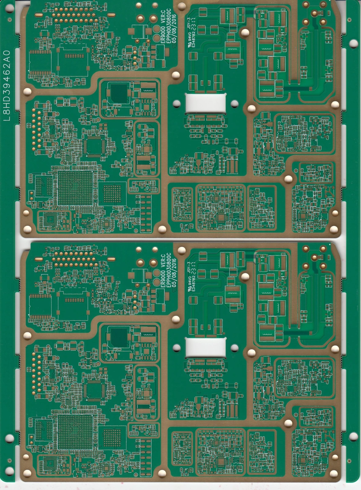
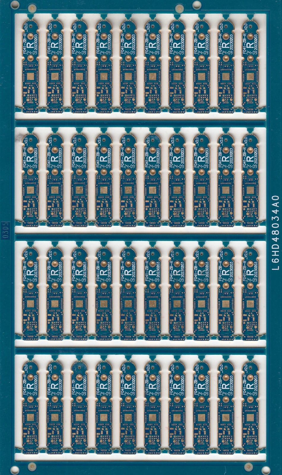
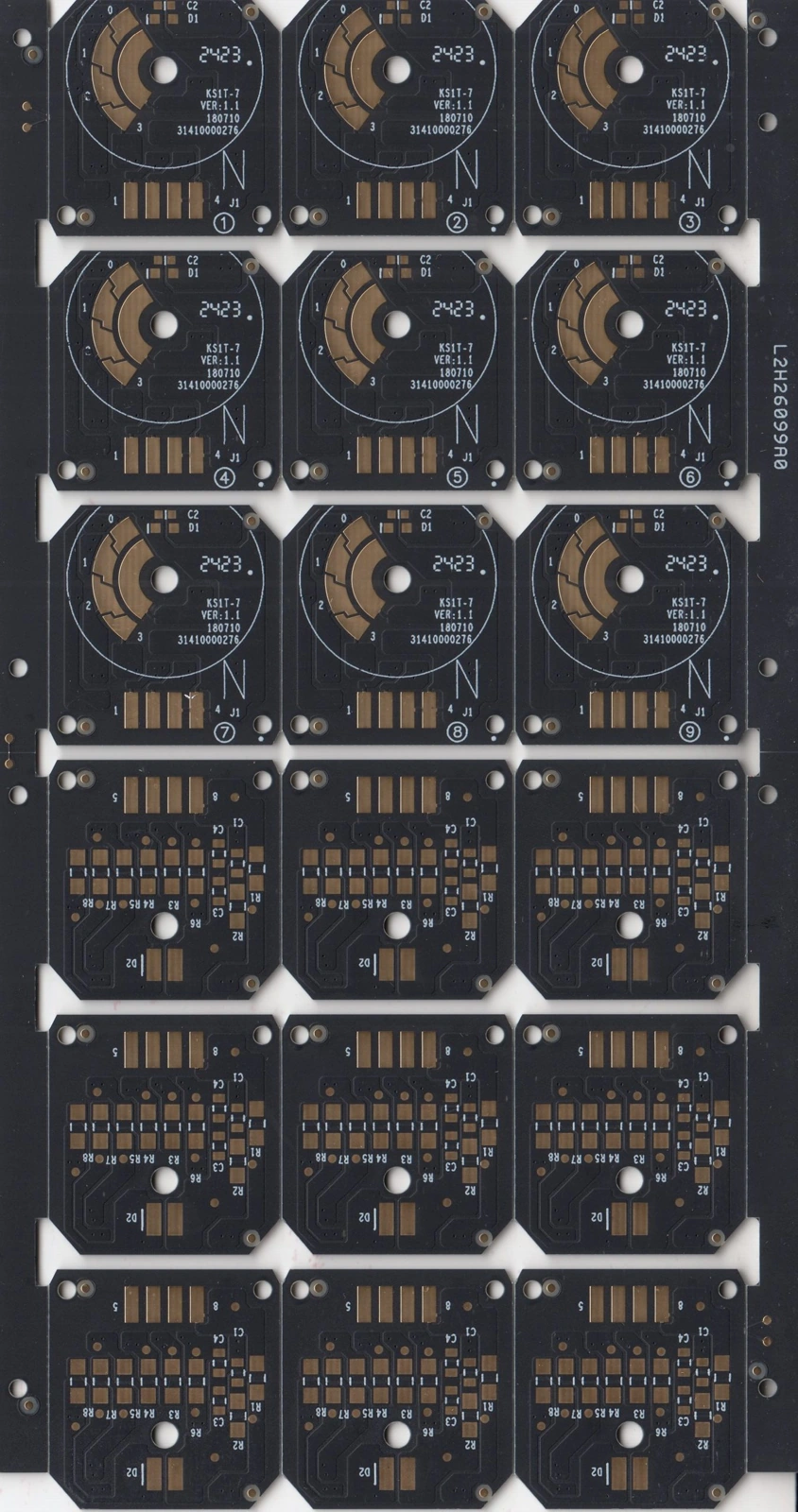
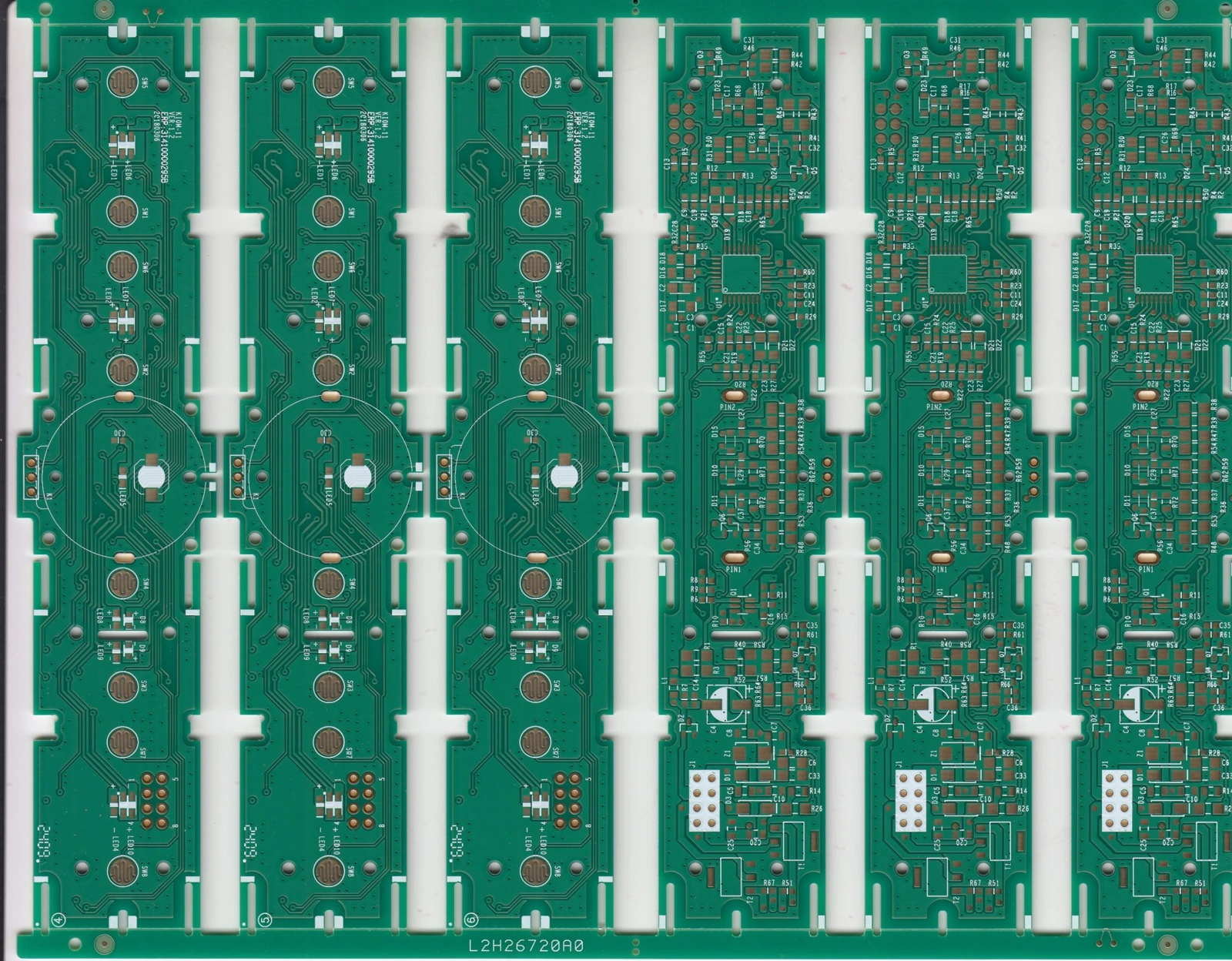
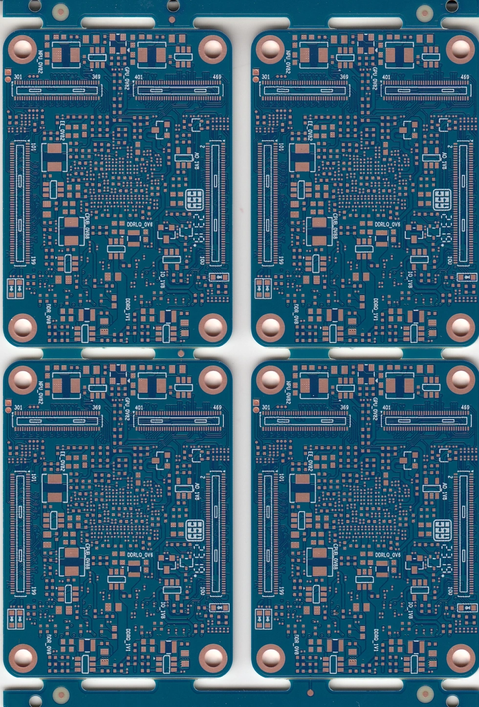
The official gallery uses JSY-007 in more than one application and JSY-018 in both server and automotive sections. An identifier alone is therefore insufficient to identify a specimen. The entries below retain the application and corresponding original bare-board image. The linked source also provides its stack diagram; no layer count, material grade or geometry is inferred from the image filename.
Industrial controls and computing
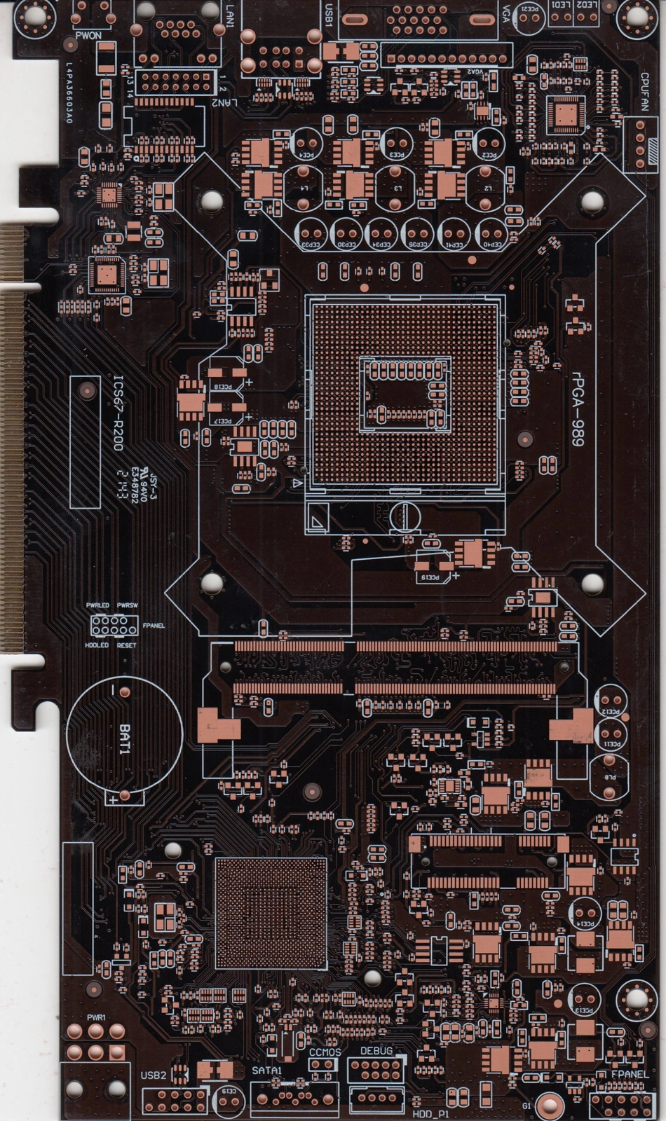
Industrial-control board · JSY-010
Official application
Industrial control
Catalogue identifier
JSY-010
Parameter scope
Group technical table is separate; specimen-specific numeric geometry not stated
Confirm isolation, copper distribution and hole definitions for the controller drawing. The published industrial example includes an original stack diagram, but does not state its laminate grade or finished-hole limit.
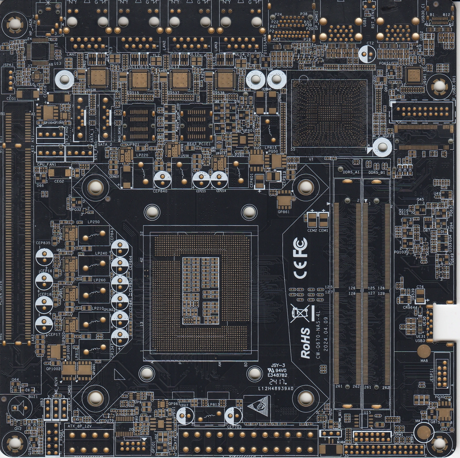
Industrial-control board · JSY-013
Official application
Industrial control
Catalogue identifier
JSY-013
Parameter scope
Group technical table is separate; specimen-specific numeric geometry not stated
Release the power and signal domains together with board thickness, copper weight and required electrical inspection. Do not substitute the group’s minimum geometry for a drawing-specific manufacturing proposal.
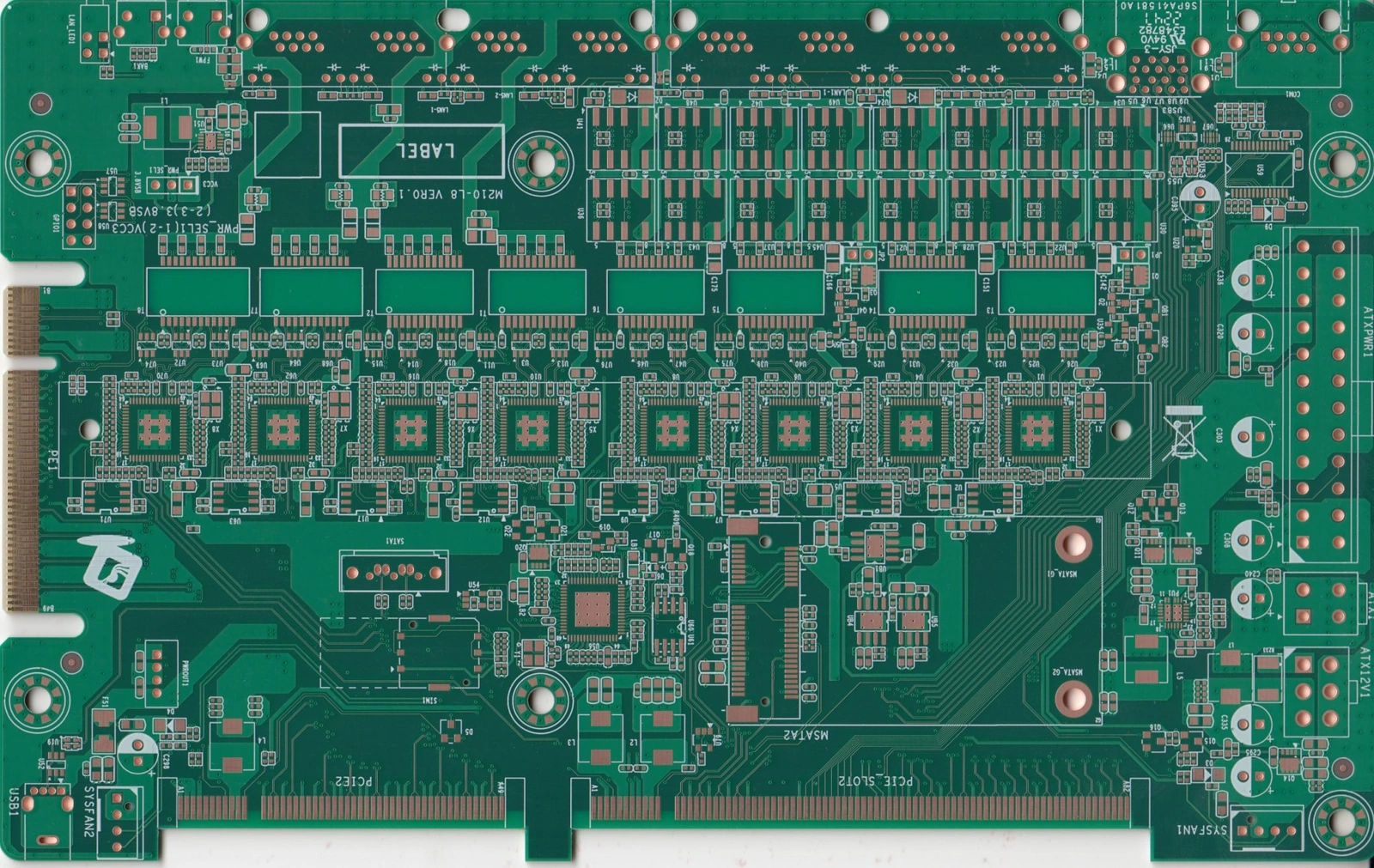
Computer board · JSY-014
Official application
Computers
Catalogue identifier
JSY-014
Parameter scope
Group technical table is separate; specimen-specific numeric geometry not stated
Supply the actual stack, dielectric grades, impedance targets and coupons. Ask which layer transitions and inspection reports are included; pad density in the photograph does not establish the finished construction.
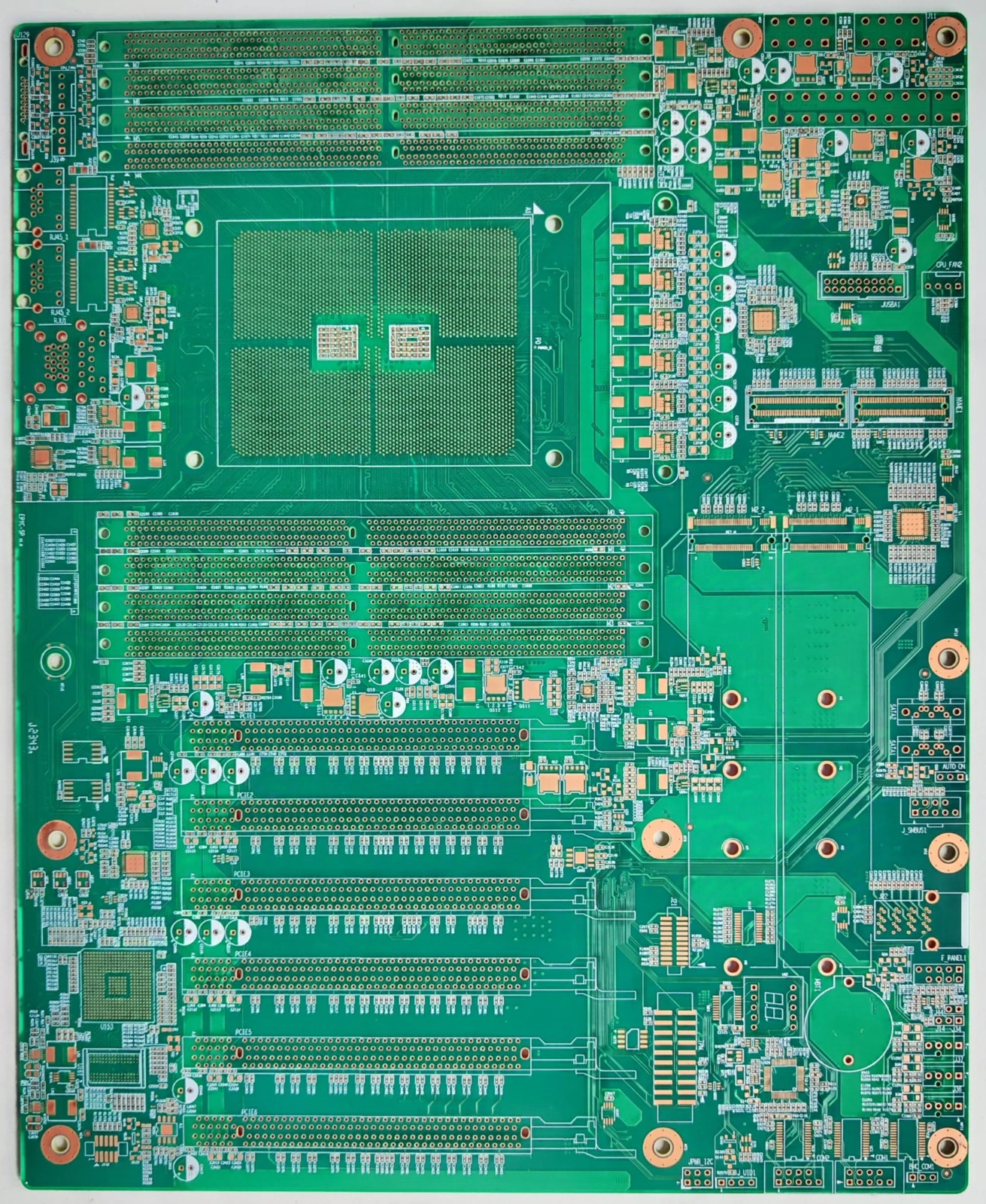
Server board · JSY-018
Official application
Servers
Catalogue identifier
JSY-018
Parameter scope
Group technical table is separate; specimen-specific numeric geometry not stated
Define the high-speed interfaces, reference planes, backdrill requirements and measurement plan. The server section and automotive section reuse JSY-018 for different illustrations; retain the application context on the quotation.
Communication interconnects
Communication board · JSY-007
Official application
Communications
Catalogue identifier
JSY-007
Parameter scope
Group technical table is separate; specimen-specific numeric geometry not stated
Specify the interconnect sequence and lamination cycles, via filling and copper-cap acceptance. JSY-007 is also used in the LED and computer galleries, so quote this communication example by application and drawing, not model number alone.
Communication board · JSY-011
Official application
Communications
Catalogue identifier
JSY-011
Parameter scope
Group technical table is separate; specimen-specific numeric geometry not stated
Submit the via map, stack and registration acceptance together. Agree cross-section sampling and electrical coverage for the released interconnection scheme rather than treating a generic HDI limit as a qualified build.
Automotive and other applications
Automotive board · JSY-018
Official application
Automotive electronics
Catalogue identifier
JSY-018
Parameter scope
Group technical table is separate; specimen-specific numeric geometry not stated
Identify the supplying site and required automotive programme documentation. Release reliability conditions, material traceability and lot records; a manufacturer-hosted IATF copy for Longyan does not qualify every site or application.
Automotive board · JSY-019
Official application
Automotive electronics
Catalogue identifier
JSY-019
Parameter scope
Group technical table is separate; specimen-specific numeric geometry not stated
Confirm the approved construction, engineering change controls and agreed testing with the manufacturing entity. Keep application suitability and qualification separate from the photograph and catalogue label.
Other-application board · JSY-006
Official application
Other applications
Catalogue identifier
JSY-006
Parameter scope
Group technical table is separate; specimen-specific numeric geometry not stated
Use the original stack diagram to discuss the interconnect architecture, then release the actual layer and via drawing. The source provides no application-specific operating conditions or material grade for this example.
The server gallery also contains a populated-system illustration. It is not used here to establish in-house assembly, component sourcing or functional test capability. The medical application tab supplied no individual board example in this review, so no medical specimen is invented.
HDI / VIA SEQUENCE, IMAGING AND COPPER
A small laser-hole value needs a complete interconnect proposal.
Published HDI characteristics
The HDI table gives a standard laser-hole diameter of 100 µm and limit of 50 µm; microvia aspect ratio 0.7:1 / 1:1; and maximum build sequence 3+N+3 / 5+N+5. Its CSP/BGA pitch row is 0.40 / 0.35 mm. These are distinct characteristics, not finished plated-hole guarantees or a qualified combination.
Stacked laser vias, filled blind holes and plugged buried holes are separately listed. Submit the via map and sequence, specify filling and cap requirements, and ask for the approved sectioning and reliability plan. The separate PCB-technology table gives impedance control ±10% / ±5%; release target impedances, frequency assumptions, coupons and acceptance with the actual stack.
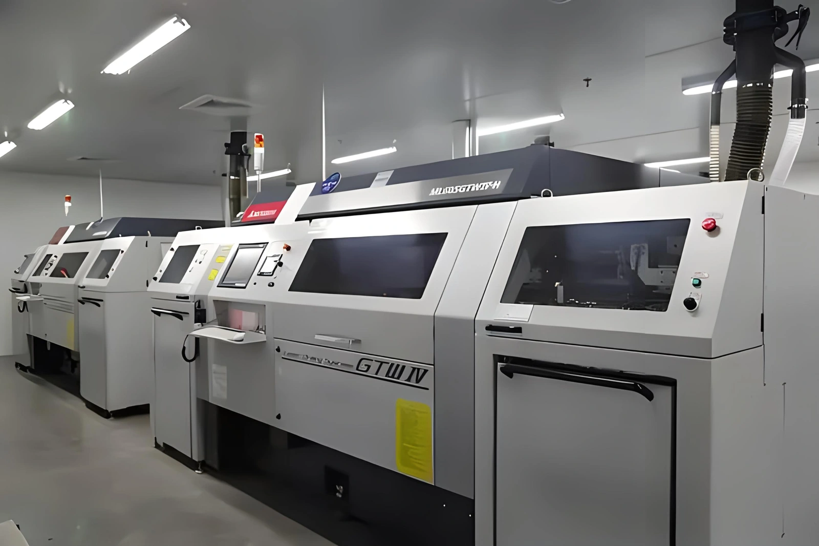
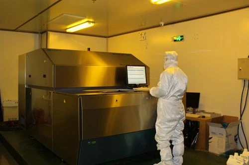
Official laser-drilling equipment photograph; machine speed, hole accuracy and producing-site allocation are not established by the photograph.
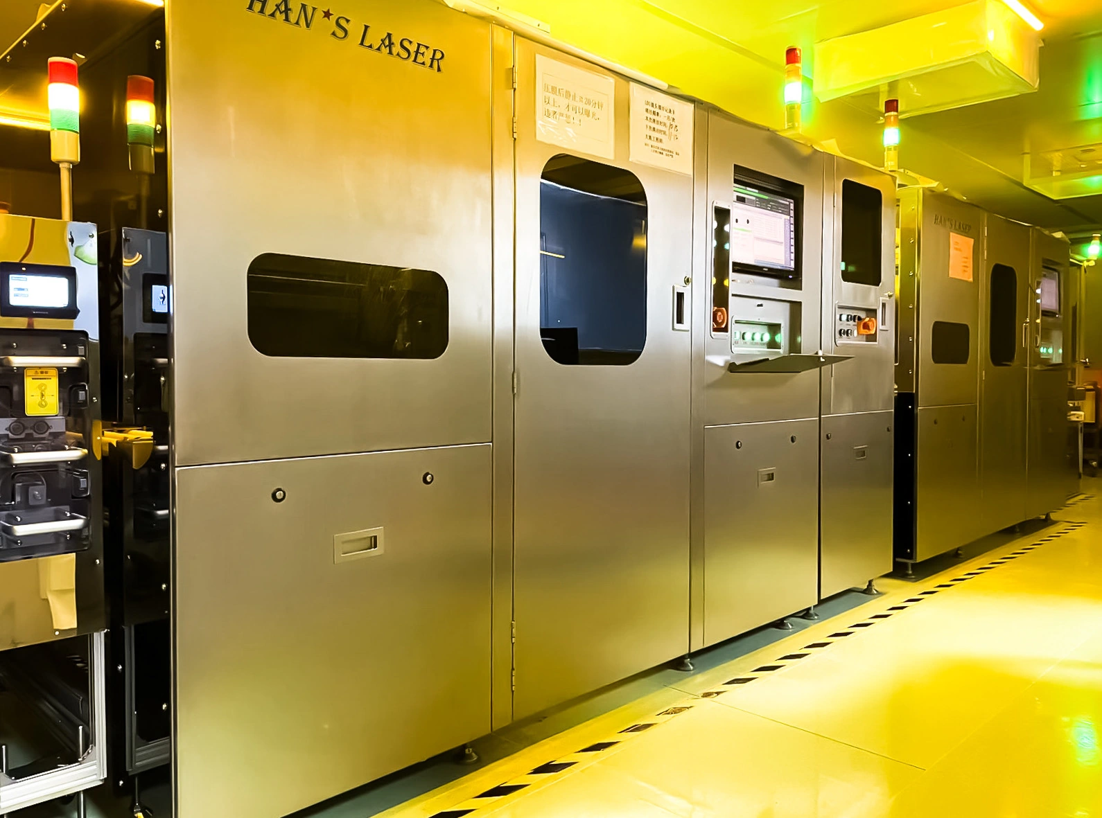
Official circuit-LDI equipment entry, distinct from the website’s solder-mask LDI entry.
Imaging is not the same process as drilling
The equipment gallery names multilayer presses, mechanical drills, circuit LDI, solder-mask LDI, VCP plating, horizontal copper deposition, laser drilling and electrical test equipment. The laser-drilling and circuit-LDI photographs show workshop equipment; other gallery entries are studio equipment illustrations and are not treated as installation evidence.
Use these process names to ask about routing and inspection. For dense interconnects, request registration criteria, copper distribution, fill/cap inspection and electrical coverage on the actual order. An equipment photograph cannot establish yield, delivered line width or reliability under your programme conditions.
Pressing, solder-mask imaging and plating photographs
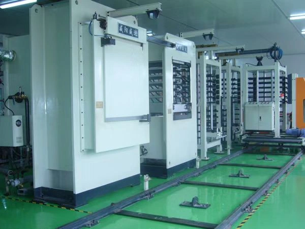
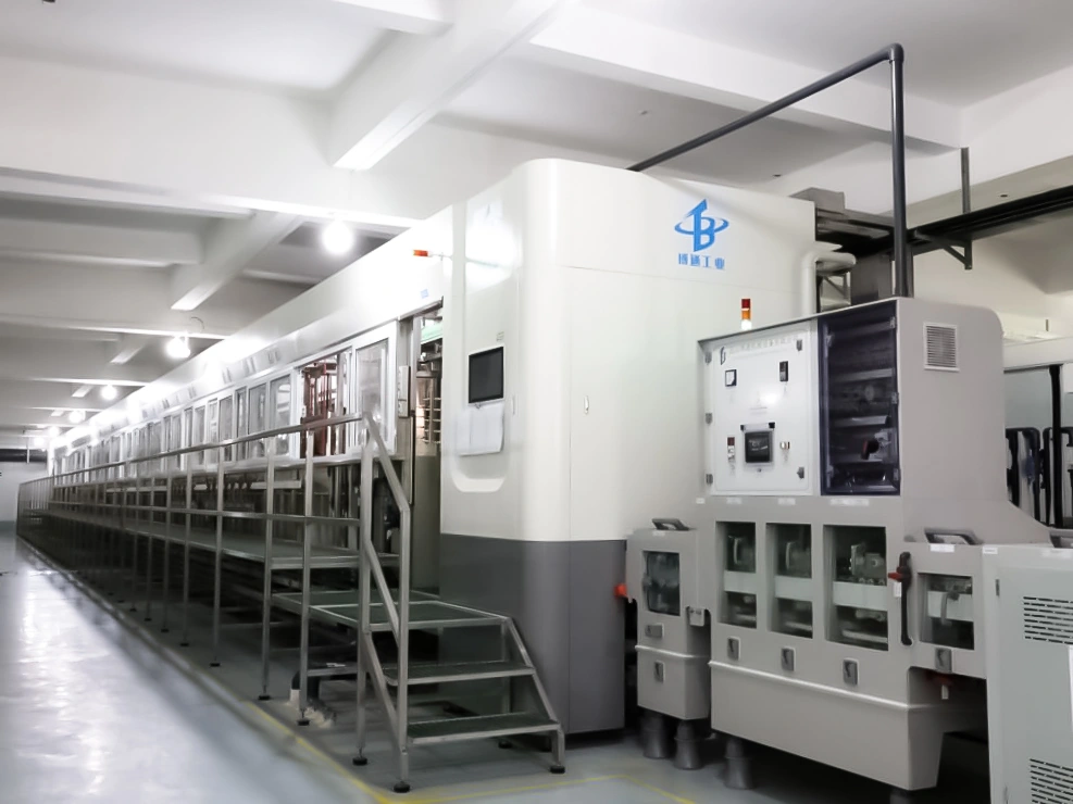
Manufacturer-labelled multilayer press from the official equipment gallery.Manufacturer-labelled solder-mask LDI entry; not a laser-drill image.Manufacturer-labelled vertical continuous plating line (VCP).
Confirm which site performs each step and which lot records accompany the shipment. No model-derived numerical specification is added from these images.
SHENZHEN / LONGYAN / PINGXIANG
The group profile is not the manufacturing contract.
Shenzhen commercial headquarters
The contact page identifies the Shenzhen entity at Yunzhi Technology Park, Building 3, Block C, Room 1508, Guangming. A Shenzhen planning-bureau notice dated 11 March 2022 lists the exact entity in an admission-qualification review for that park. This is historical entity context, not PCB quality approval or proof of current occupancy.
Longyan production
The company describes the Longyan base as operating from 2010 and positions it for first-, second- and third-order HDI, including LED displays, communications and consumer electronics. Its Longyan qualification copies identify a specific legal holder and Wuping addresses; match those documents to the producing location on the quotation.
Pingxiang phase allocation
The current site card assigns phase-one 4–16-layer through-hole boards and phase-two HDI. The site card gives 2022 as establishment; the timeline says phase one operated in 2024; the introduction says 2025 operation. These descriptions are not reconciled into one commissioning date or a promise that every phase is currently available.
Ask the seller to identify the contracting company, producing plant, subcontracted steps if any, and approval route for transferring the order between sites. Current throughput, spare capacity and lead time require an order-specific confirmation; group descriptions do not reserve a production slot.
QUALIFICATION / HOLDER, DATE AND SCOPE
Read the document against the site and construction.
Longyan automotive-system copy
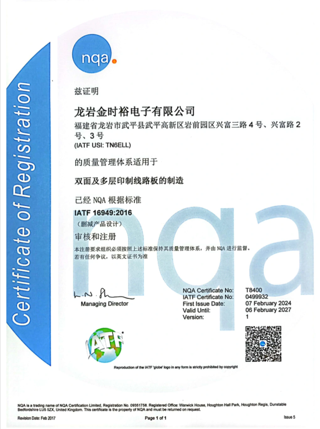
The manufacturer-hosted NQA document T8400 / IATF 0499932 names Longyan Jinshiyu and Wuping addresses. It shows 7 February 2024 to 6 February 2027 and covers double-sided and multilayer PCB manufacturing, excluding product design. This is a reviewed website copy; current issuer status was not independently established, and it is not a certificate for the Shenzhen or Pingxiang entity.
Dated UL construction copy
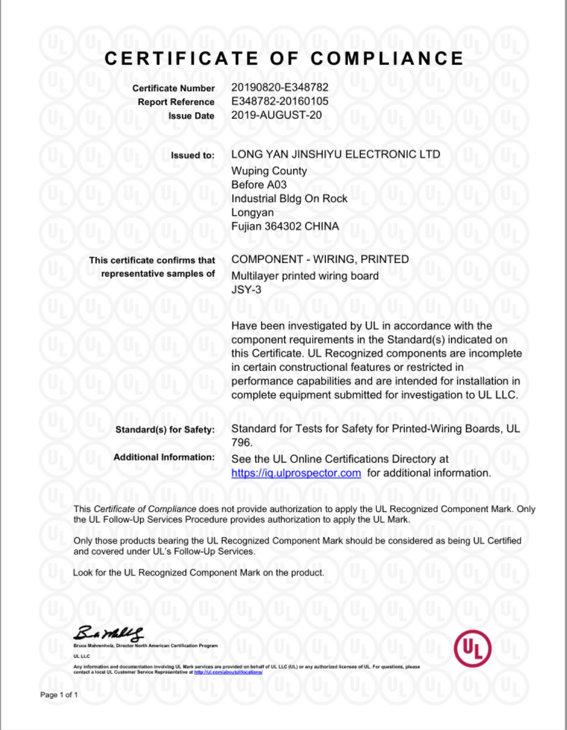
The 20 August 2019 copy names LONG YAN JINSHIYU ELECTRONIC LTD, file E348782 and representative multilayer construction JSY-3 under UL 796. It does not establish approval of every gallery board. The official registry requires sign-in; current ownership, follow-up scope and your proposed materials need a current record.
ISO and submitted-sample report
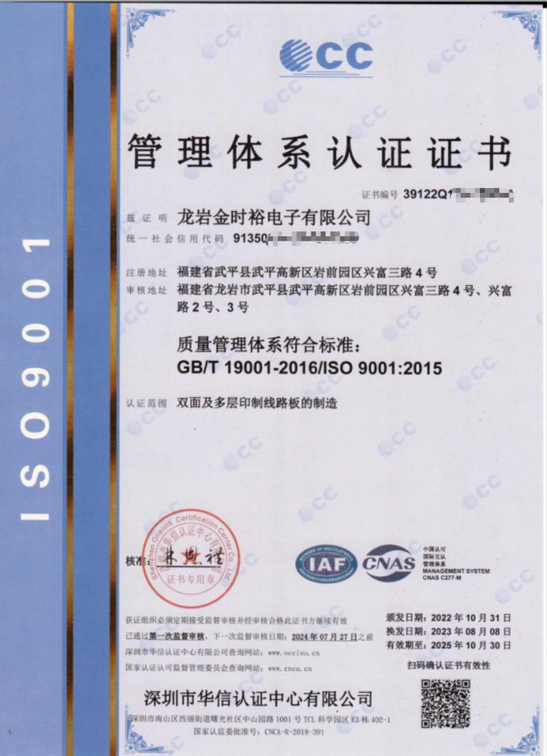
The ISO 9001 copy reviewed here expired on 30 October 2025; its certificate number is partly masked. It is not displayed as a current certification badge.
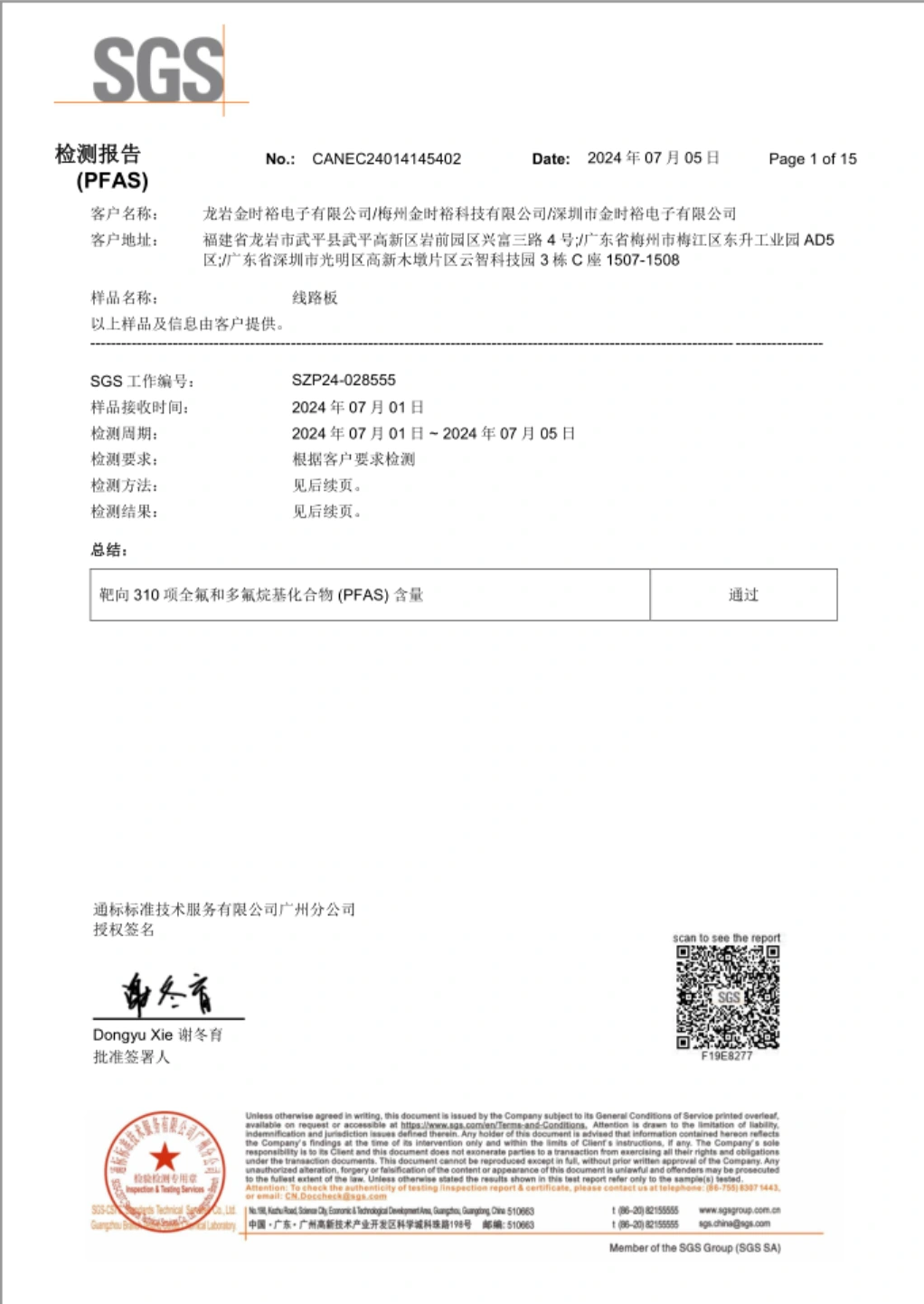
SGS report CANEC24014145402, dated 5 July 2024, supplies page 1 of 15 and states a submitted circuit-board sample passed a targeted 310-PFAS test. The test methods and detailed results point to following pages, which are not supplied in this image. This is not a universal “PFAS-free” statement for all materials, batches or sites.
View the corresponding manufacturer-hosted document copies
Longyan NQA/IATF copy: manufacturing scope excludes product design; current issuer status requires confirmation.Dated UL E348782 copy: representative JSY-3 construction under UL 796.Expired ISO 9001 copy; masked identifiers are not reconstructed.SGS submitted-sample PFAS report, page 1 of 15 only.
ENGINEERING RELEASE / ONE APPROVED CONSTRUCTION
Ask for a site-specific response to your drawing.
Architecture: revision, stack, via sequence, dielectric grades and lamination cycles; include the application context if referencing a gallery code.
Geometry: finished copper and line definitions, drill tool versus finished hole, panel arrangement, outline and mask registration.
Electrical acceptance: impedance targets and coupons, netlist coverage, microsections and agreed reliability tests.
Qualification: supplying entity and site, current holder/scope records, traceability and programme-specific approval documents.
Commercial release: quantities, pilot-to-volume transition, actual production slot and change-control responsibilities.
Reviewed 9 October 2026 using the company, contact, technical tabs, individual application galleries, original equipment and document images, and the original Shenzhen public notice. Catalogue specimens remain separate from group-wide processing limits.
SOURCE TRAIL
Sources behind this profile
Individual review dated 9 October 2026. Standard and limit columns retain their copper and process conditions. Historical document copies are separated from current issuer checks; the Shenzhen admission notice relates to headquarters, not Longyan factory quality.