TAIZHOU JINDING / THREE DIFFERENT ENGINEERING CONVERSATIONS
Start with the electrical, contact or thermal job the board must do.
Jinding’s official catalogue is organised around finishes and constructions: immersion gold, pure tin, anti-oxidation, aluminium base and gold-finger cards. Its six photographed products give a useful starting point for a sourcing brief, but do not provide a numerical fabrication capability sheet. This review follows the actual examples instead of attaching a generic layer, hole or impedance envelope to them.
The company introduction describes high-frequency single / double-sided and multilayer boards, FR-4 single / double-sided and multilayer boards, and aluminium-base boards. It does not state a maximum layer count, minimum trace / space, minimum finished hole, impedance tolerance or material-grade list. Those values remain drawing-specific questions rather than invented filter entries.
RF AND SOLDERABLE PADS / MATERIAL GRADE BEFORE MASK COLOUR
The high-frequency reference needs a defined dielectric and test plan.
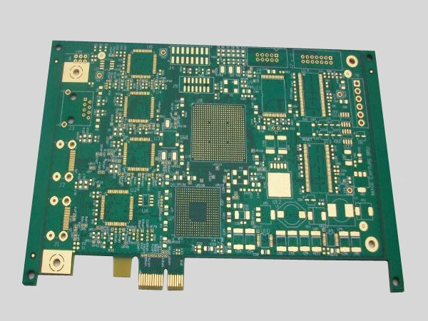
Corresponding original manufacturer image, shown whole. No dimensions or process limits are inferred from its appearance.
High-frequency immersion-gold PCB reference
Official product family
高频沉金板 — manufacturer high-frequency immersion-gold category. Exact laminate and frequency band are not published.
Layers / trace / finished hole
Not specified for this photographed board
Order acceptance
Specify laminate brand and grade, dielectric thickness, design versus process Dk, operating band, stack, copper and controlled-impedance coupon. Have the factory accept the RF construction and finish together; the image is not a measured loss or impedance result.
Specify the RF stack
The title identifies a high-frequency immersion-gold board. It does not name Rogers, PTFE, a ceramic-filled laminate or a particular frequency band. Provide the exact approved grade, dielectric thickness, copper, stack and the operating band. Agree the Dk value and method used for the impedance design; a laminate data-sheet value and the effective design value should not be assumed identical.
Specify what will be measured
If controlled impedance or RF loss is required, request the coupon design, measurement method, acceptance limits and report. The gallery’s flying-probe and high-voltage testers answer different questions; their presence is not an RF loss, impedance or signal-integrity result for this example.
Two other soldering routes in the catalogue
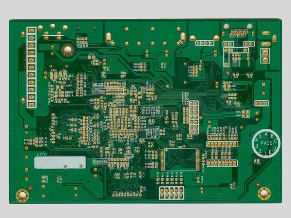
Corresponding original manufacturer image, shown whole. No dimensions or process limits are inferred from its appearance.
Immersion-gold green-board reference
Official product family
沉金板 — immersion-gold catalogue board; nickel / gold thickness and exact process are not quantified.
Layers / trace / finished hole
Not specified for this photographed board
Order acceptance
Agree nickel and gold deposits, flatness, pad solderability, storage and reflow requirements. If the project requires ENIG to a named specification, state it explicitly rather than accepting a colour or category label.
Corresponding original manufacturer image, shown whole. No dimensions or process limits are inferred from its appearance.
FR-4 anti-oxidation panel reference
Official product family
FR4抗氧化板 — FR-4 and anti-oxidation are named by the product title. Exact laminate grade and coating chemistry are unspecified.
Layers / trace / finished hole
Not specified for this photographed board
Order acceptance
Specify the FR-4 grade, copper and mask, then ask whether the quoted anti-oxidation route is OSP, its supplier/process control, storage condition and permitted assembly reflow cycles.
“Immersion gold” does not supply nickel / gold thickness or a named ENIG specification. “FR-4 anti-oxidation” supplies a substrate family and finish description, but does not identify the coating chemistry or guarantee a particular number of reflow cycles. Ask Jinding to identify the exact quoted finish, storage conditions and solderability acceptance.
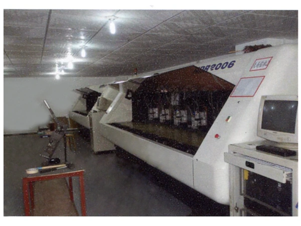
The navigation also lists pure-tin boards, and the equipment gallery labels a lead-free hot-air-solder-leveling line. No individual pure-tin product specification is supplied by the reviewed listings. An installed-line photograph is not a statement that every tin product follows that route.
GOLD-FINGER CARD / CONTACT LIFE IS A SEPARATE FINISH REQUIREMENT
Write the mating interface before agreeing the gold finish.
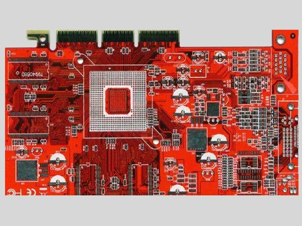
Corresponding original manufacturer image, shown whole. No dimensions or process limits are inferred from its appearance.
Gold-finger card — red catalogue reference
Official product family
金手指卡板 — edge-card product category; contact plating type, hardness and thickness are unspecified.
Layers / trace / finished hole
Not specified for this photographed board
Order acceptance
Provide connector mating dimensions, contact wear cycles, selective hard-gold requirements if applicable, nickel barrier, bevel angle and tolerance. Immersion gold and a wear-resistant contact finish are separate decisions.
Contact surface
State the mating cycles, selective plating area, required hardness and minimum deposit thickness, with a nickel barrier requirement where applicable. The catalogue does not specify these values. Do not treat immersion gold on solder pads as a substitute for a wear-qualified edge-contact finish.
Mechanical fit
Supply the connector manufacturer’s card thickness, pad spacing, edge setback, bevel geometry and insertion datums. Confirm plating coverage around the bevel and the inspection method. No bevel angle or outline tolerance is calculated from the red board’s photograph.
Lot release
Agree dimensional inspection, deposit measurement, adhesion acceptance and traceability to the released revision. If the connector interface needs a durability qualification, identify the test and responsibility separately from routine bare-board electrical testing.
ALUMINIUM-BASE EXAMPLES / THE BOARD AND HOUSING FORM ONE THERMAL PATH
Define the insulation and mounting interface as carefully as the copper.
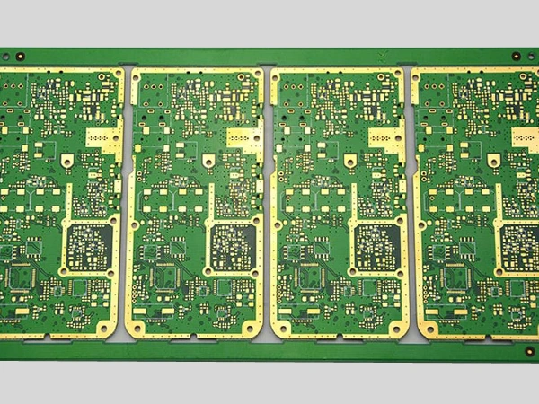
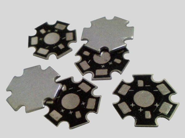
Corresponding original manufacturer image, shown whole. No dimensions or process limits are inferred from its appearance.
Aluminium-base boards — shaped front / back reference
Official product family
铝基板 — the title identifies aluminium base. Exact base alloy, dielectric and thermal properties are unspecified.
Layers / trace / finished hole
Not specified for this photographed board
Order acceptance
Define the base alloy and thickness, dielectric thermal data and withstand test, copper, flatness, mounting datums and thermal-interface contact. Confirm front / back and outline in the controlled drawing.
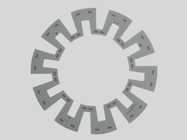
Corresponding original manufacturer image, shown whole. No dimensions or process limits are inferred from its appearance.
Aluminium-base ring reference
Official product family
铝基板 — ring-shaped catalogue reference. Dimensions, stack and LED assembly are not published.
Layers / trace / finished hole
Not specified for this photographed board
Order acceptance
Provide ring inner / outer diameters, slot geometry, screw clearances, dielectric, copper and the thermal path into the housing. Clarify bare-board versus populated assembly scope; visible pads do not establish assembly service.
01 / CIRCUIT
Copper and dielectric
Specify circuit copper, dielectric thickness, thermal property and test method, working voltage and insulation acceptance. The aluminium-base title does not establish a thermal-conductivity number, breakdown voltage or a recognised material grade.
02 / BOARD
Base and outline
Specify alloy, base thickness, flatness, deburring, holes and slot dimensions. The shaped front / back image and ring image are separate catalogue examples. Neither includes a scaled mechanical drawing or an approved mounting pattern.
03 / HOUSING
Thermal contact
Define the interface material, pressure or fastener arrangement and the surface that contacts the housing. Agree whether inspection covers the bare board alone or the assembled thermal path. Pads visible in an image do not establish that Jinding supplies populated LED assemblies.
LABELLED ORIGINAL GALLERY / MACHINING, PLATING AND IMAGING
Ask which route and assets will make the released revision.
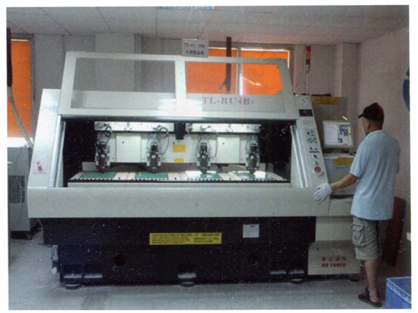
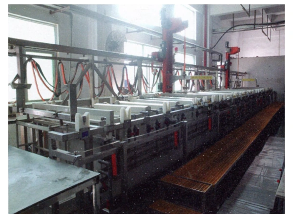
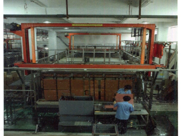
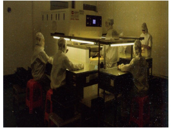
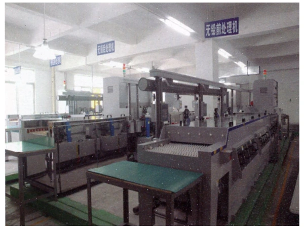
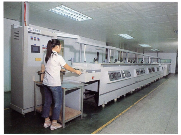
Official gallery: CNC drilling machine. No drill diameter, machine count or calibration date is provided.Official gallery: CNC edge-milling machine. Agree the finished outline tolerance and datums.Official gallery: automatic electroless-copper line. This image is not a plated-wall thickness report.Official gallery: automatic electroplating line. Confirm the stack and contact-plating route for the order.Official gallery: parallel exposure machine. No minimum trace / space or LDI capability is inferred.Official gallery: lead-free hot-air-solder-leveling equipment, as labelled by the manufacturer.Official gallery: anti-oxidation line. The photograph does not identify coating chemistry or permitted reflow cycles.
The first gallery page also labels a laminating-film machine, developer, alkaline etcher, press, anti-oxidation line and ovens. The second page adds a magnifier and pH meter. The 18 named images are manufacturer disclosures, without an installed-machine register, current quantities or inspection date.
The “film laminating” photograph concerns imaging-film preparation; it is not sufficient evidence of a multilayer-stack lamination press. For a high-frequency multilayer job, request the actual lay-up / lamination route, material handling and any subcontracted step. No laser-drilling, HDI or rigid-flex qualification is added from this gallery.
OPTICAL, ELECTRICAL AND MATERIAL CHECKS / DIFFERENT OUTPUTS
Turn the inspection photographs into an agreed shipment record.
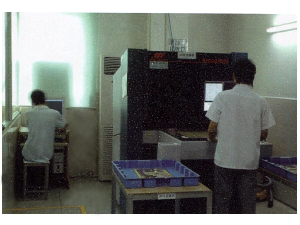
Manufacturer-labelled AOI tester. Optical inspection does not replace the order’s netlist test.
Optical comparison
Identify the reference artwork and inspection coverage, handling of defect dispositions and traceability to the fabrication revision. A photograph does not reveal the configured inspection thresholds.
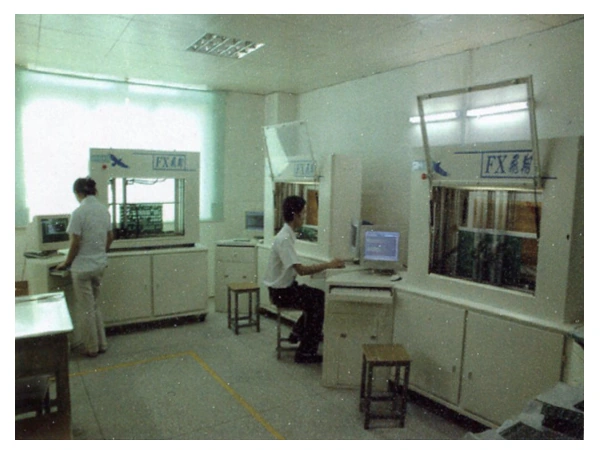
Manufacturer-labelled flying-probe testers. Test coverage and limits remain order-specific.
Continuity and isolation
Provide the netlist and ask which flying-probe or fixture method is used for the lot, its test limits and the report supplied. Bare-board test is separate from functional testing of a populated assembly.
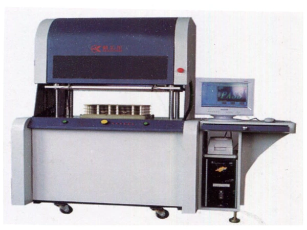
Manufacturer-labelled high-voltage tester. No test voltage is assigned to a catalogue board.
Withstand requirements
State the voltage, dwell, leakage limit and sampling for the intended construction. A high-voltage test requirement must be accepted for the exact dielectric and spacing, especially on the aluminium-base examples.
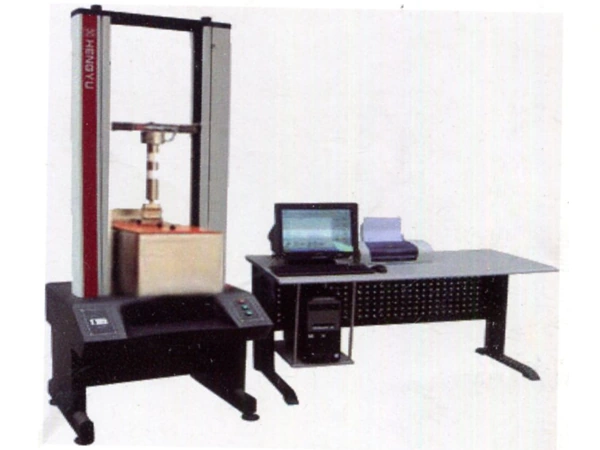
Manufacturer-labelled copper-foil tensile tester. A displayed instrument is not a material-lot result.
Material and interface evidence
Agree the laminate / foil lot documentation and the adhesion or mechanical test required. This tensile tester is not evidence of an order’s thermal conductivity, gold deposit, impedance or calibration status.
YONGANZHOU, TAIZHOU / HISTORICAL NAME MATCH AND CURRENT ORDER IDENTITY
The official site and a Jiangsu original record name the same company.
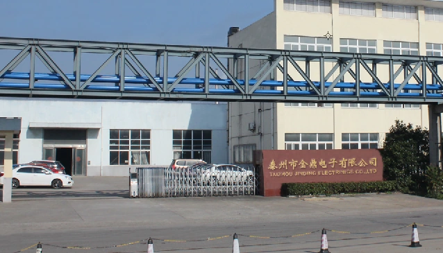
Original company-page factory photograph, with 泰州市金鼎电子有限公司 on the sign. The picture is not a current site audit.
Published production contact
The site names 泰州市金鼎电子有限公司, Taizhou Jinding Electronics Co., Ltd., at Gaoyong Pharmaceutical Industrial Park, Yonganzhou, Gaogang, Taizhou, Jiangsu. It publishes 0523-86927508 / 0523-86928858 and jindingdzpcb@jindingdz.cn.
The domain mailbox is disclosed by the official contact page. Mailbox control has not been tested and no external inquiry has been sent during this review. Confirm the contracting and invoicing entity, producing address and engineering responsibility before releasing an order.
The introduction dates founding to October 2009. Its capacity statement explicitly refers to an early annual production capacity of about 500,000 m²; it is not current available capacity or a promised delivery slot.
Jiangsu’s dated credit-management notice
The Jiangsu Department of Industry and Information Technology’s original notice, published 22 January 2014, lists 泰州市金鼎电子有限公司 in the Taizhou section of the 2013 second-batch credit-management standardisation acceptance list. This supports a historical legal-name match. It is not a current credit rating, an independent factory audit or a PCB qualification.
The company copy states 40 mu of land and 20,000+ m² of factory buildings, but another homepage advantage block says 30 mu and the company-page numerical label calls 20,000 m² land area. The reviewed sources do not resolve those scope differences. Request a current site and equipment schedule where capacity matters.
The listed application sectors include aerospace, microwave communications, industrial control and automotive electronics. These sector descriptions do not establish IATF, aerospace, military or UL qualification. No current scoped issuer record or product-construction annex is provided by the reviewed pages.
SUPPLIER RESPONSE / ACCEPT THE DRAWING BEFORE COMPARING PRICE
Ask for one marked-up engineering acceptance and a defined shipment package.
Choose the matching route: RF immersion gold, solderable FR-4, wear-qualified edge card or aluminium-base thermal construction.
Release the construction: exact material grade, stack, finished thickness and copper, trace / space, finished holes and dimensions. Unpublished limits need explicit engineering confirmation.
Resolve the interface: solder finish and assembly conditions, contact plating and bevel, or thermal dielectric and housing interface.
Agree production and inspection: producing site, outsourced operations, artwork / netlist reference, optical and electrical tests, material trace and required reports.
Agree commercial release: current quantity, first / repeat-order approval, lead-time start, shipping scope and current qualification records required by the application.
Reviewed 9 October 2026. Six independently mapped catalogue photographs are selectable on the existing factory URL. Only explicitly named FR-4 and aluminium-base material families are recorded; unreported geometry and performance stay unknown.
Each product title, corresponding original image, both equipment-gallery pages and the Jiangsu government original were reviewed separately. Unrelated steel-material boilerplate in the manufacturer’s page header is excluded from this PCB profile.