HUABANGXIN / RF AND MICROWAVE BARE-BOARD MANUFACTURING
Choose the laminate and stack before choosing a microwave application label.
Huabangxin describes a Shenzhen business focused on printed circuits associated with RF and microwave devices. Its catalogue gives useful individual builds for power dividers, antennas, amplifiers and combiners. The procurement task is to turn those examples into a controlled laminate, copper, finish and mechanical drawing, then specify what will actually be measured.
Nine references below retain their corresponding original catalogue images and their own parameter fields. The double-sided 0.8 mm OSP power-divider reference already listed on PCBVerified remains the same product. Its material field names a function rather than a grade; its appearance and category cannot fill that gap.
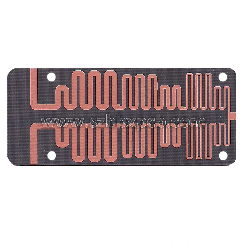
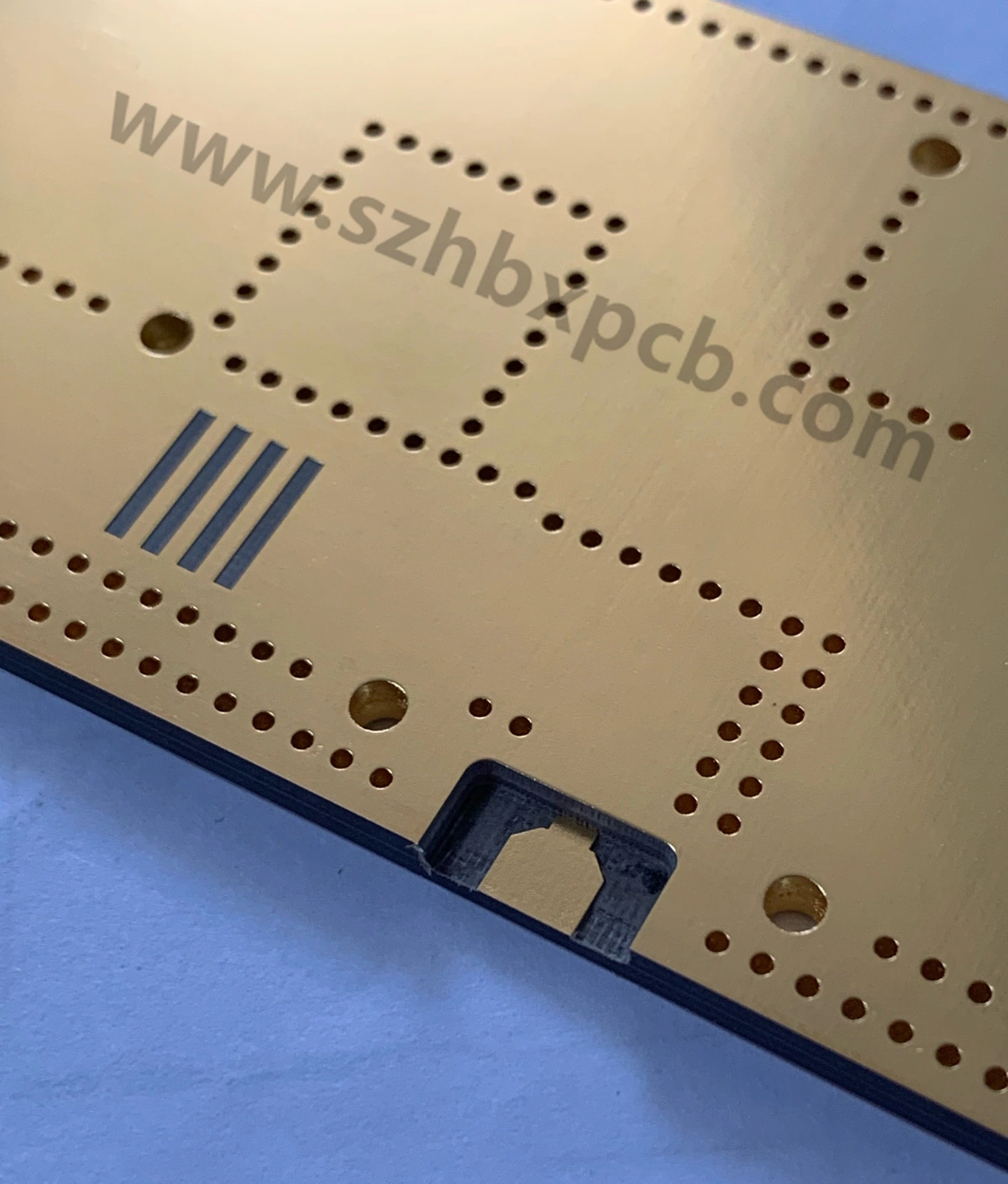
Whole corresponding manufacturer catalogue photograph. Board dimensions and measured RF performance are not inferred from the image.
Two-way RF power-divider PCB
Published construction
Laminate grade not supplied · 2 layers
Board thickness
0.8 mm
Copper / finish
1 oz / OSP
Mask / legend
Neither supplied on this example
The catalogue names a two-way power divider but repeats the application in its material field; it supplies no laminate grade, frequency band, isolation or insertion-loss result.
Engineering response: Define laminate grade, substrate tolerance, copper, launches, port impedance and S-parameter / isolation acceptance with the assembly or enclosure boundary.
MATERIAL IDENTITY / KEEP EACH CATALOGUE BUILD SEPARATE
RO3010 is explicit; the antenna record says Rogers4003 without a suffix.
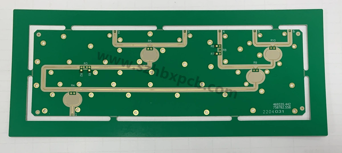
Whole corresponding manufacturer catalogue photograph. Board dimensions and measured RF performance are not inferred from the image.
RO3010 double-sided PCB
Published construction
Rogers3010 — manufacturer material field · 2 layers
Board thickness
0.508 mm
Finish / mask / legend
Immersion gold / green / white
Copper
Not stated on this specific reference
The title explicitly identifies a double-sided RO3010 board. Its own page supplies 0.508MM, green mask, white legend and immersion gold; copper weight is not stated.
Engineering response: Specify grade and revision, laminate batch trace, copper construction, actual dielectric thickness and mask keep-outs; agree the RF coupon and measurement method.
What the laminate maker establishes
Rogers’ own RO3010 page identifies a ceramic-filled PTFE laminate. That independently supports the material-family description. It does not establish that a Huabangxin shipment uses a genuine Rogers lot or meets your finished-circuit loss target. Obtain the order’s exact grade, thickness / copper designation, lot identifiers and procurement trace.
The manufacturer’s separate RO3010 catalogue page omits a unit after “0.508.” The double-sided reference shown here explicitly writes “0.508MM”; that is why its own thickness can be recorded in millimetres. Values from one record are not used to silently repair another.
Whole corresponding manufacturer catalogue photograph. Board dimensions and measured RF performance are not inferred from the image.
Rogers4003 antenna PCB
Published construction
Rogers4003 — suffix not supplied · 2 layers
Board thickness
0.762 mm
Copper / finish
1 oz / OSP
Mask / legend
Neither supplied on this example
The manufacturer writes Rogers4003, without the C suffix, and explicitly lists a double-sided antenna board. No radiation pattern or measured frequency band is supplied.
Engineering response: Resolve the exact laminate grade and design-Dk basis, copper roughness, antenna stack and dimensional controls; agree return loss and radiation tests only if included in supply.
Rogers4003 on this antenna page should not be automatically expanded to RO4003C. The general company introduction lists RO4003C, but does not resolve the designation on this particular reference. Ask the factory to return the full material code and current datasheet with the proposed stack. Define whether the requested dielectric constant is a design value or a value from a specified test method.
TACONIC REFERENCES / THICKNESS AND FINISH FOLLOW THE ACTUAL BOARD
Two RF-35 boards have different stacks; TLX-8 is another material choice.
RF-35 amplifier
1.016 mm · 1 oz · immersion gold. No solder mask or legend in the published example.
RF-35 antenna
0.508 mm · 1 oz · OSP. The same material name does not make these builds interchangeable.
TLX-8 combiner
2.0 mm · 1 oz · immersion gold. The record does not publish measured combiner isolation or loss.
Whole corresponding manufacturer catalogue photograph. Board dimensions and measured RF performance are not inferred from the image.
RF-35 power-amplifier PCB
Published construction
Taconic RF-35 · 2 layers
Board thickness
1.016 mm
Copper / finish
1 oz / immersion gold
Mask / legend
Neither supplied on this example
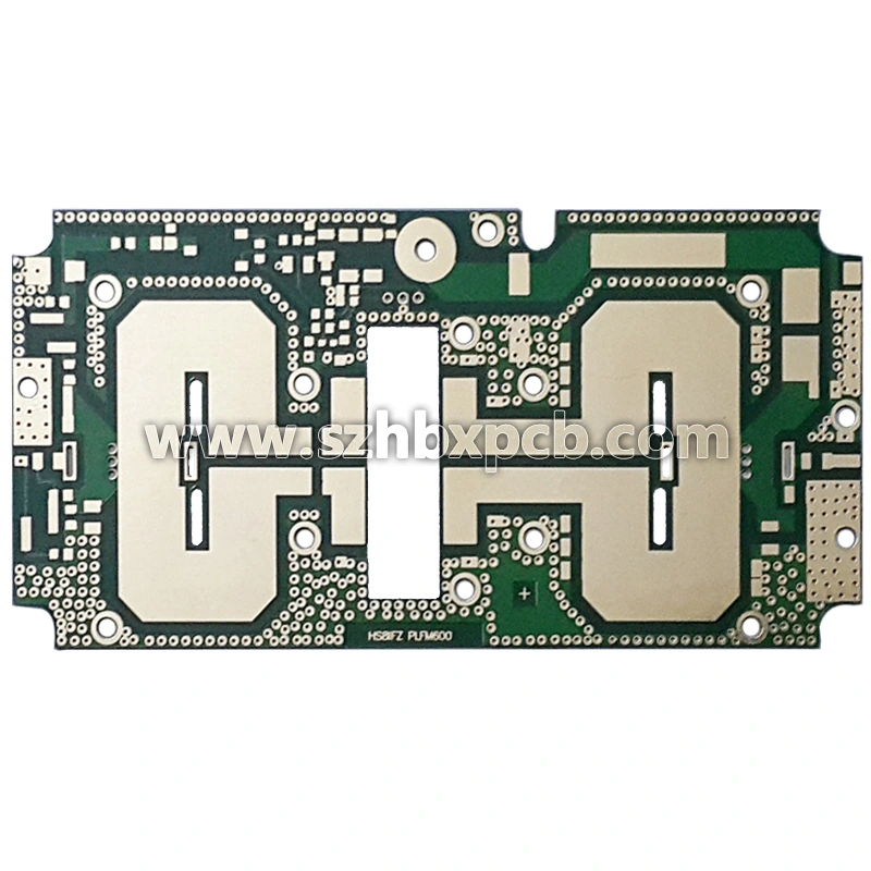
This RF-35 amplifier-board reference is a bare PCB with published construction fields; power, gain, active-device choice and complete-amplifier test results are not supplied.
Engineering response: Release the RF and thermal stack, copper / finish, device interface and grounding; define bare-board electrical testing separately from amplifier gain and output-power testing.
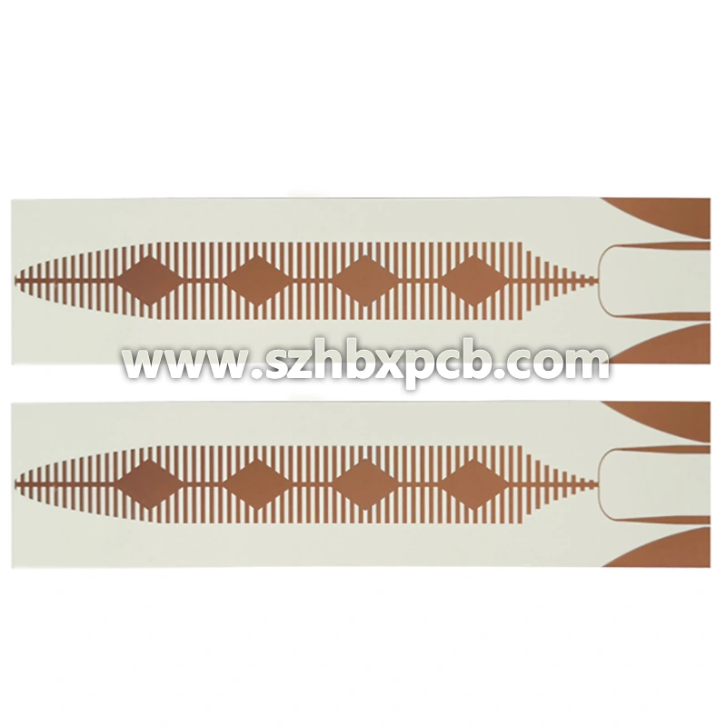
Whole corresponding manufacturer catalogue photograph. Board dimensions and measured RF performance are not inferred from the image.
RF-35 antenna PCB
Published construction
RF-35 — official antenna reference · 2 layers
Board thickness
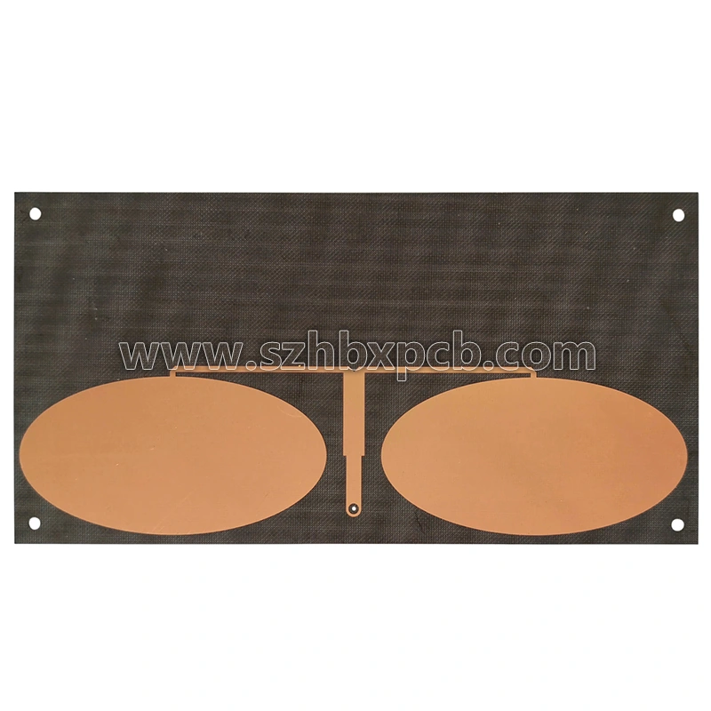
0.508 mm
Copper / finish
1 oz / OSP
Mask / legend
Neither supplied on this example
A separate RF-35 antenna reference uses 0.508 mm and OSP, unlike the 1.016 mm immersion-gold amplifier reference. These are different catalogue builds.
Engineering response: Specify the antenna dielectric and copper tolerances, treatment and storage / assembly window for OSP, launches and the actual RF measurement boundary.
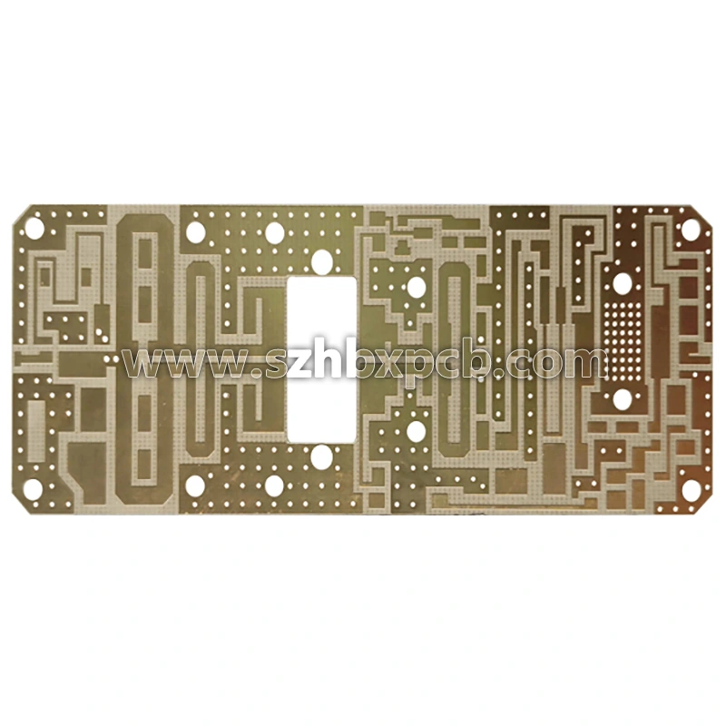
Whole corresponding manufacturer catalogue photograph. Board dimensions and measured RF performance are not inferred from the image.
TLX-8 microwave-combiner PCB
Published construction
TLX-8 · 2 layers
Board thickness
2.0 mm
Copper / finish
1 oz / immersion gold
Mask / legend
Not stated on this specific reference
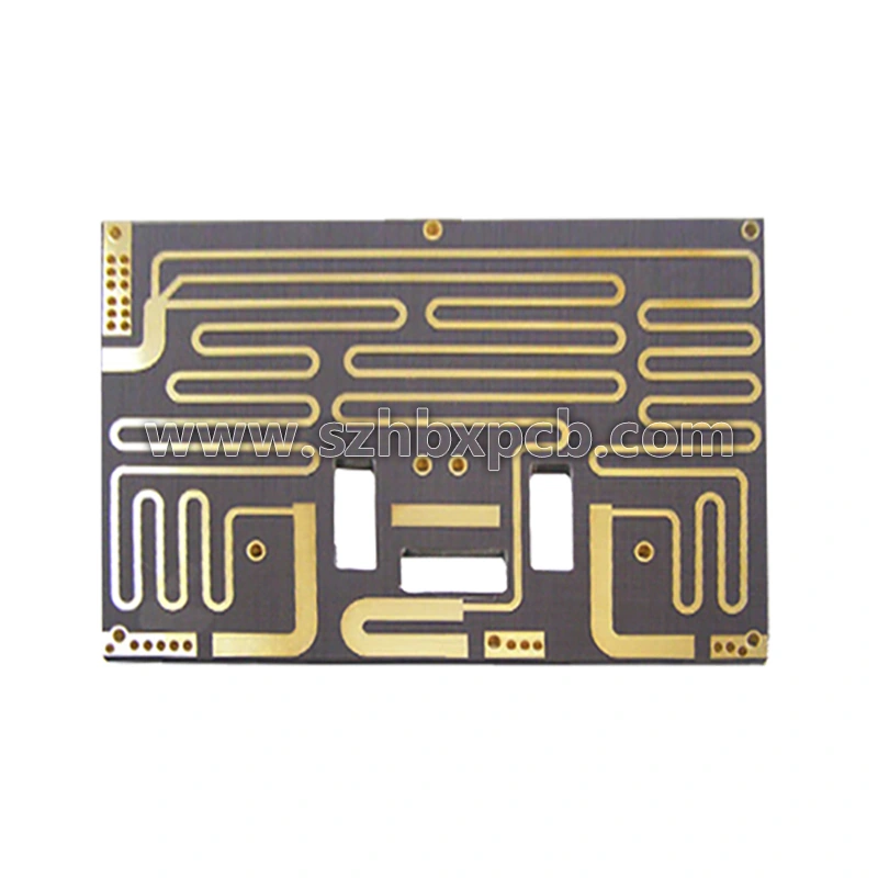
The official title and material field name a TLX-8 combiner board, with double-sided construction, 2.0 mm thickness, 1 oz copper and immersion gold. No combiner performance is measured on the page.
Engineering response: Define ports, frequency, copper, substrate and launched stack; agree insertion loss, isolation and power-handling test responsibility rather than assigning ratings from the title.
The catalogue’s “power amplifier” and “combiner” names identify PCB applications. Huabangxin’s introduction also lists many associated RF devices and adapters; that list is not proof that the company supplies a complete calibrated adapter, powered amplifier or qualified RF assembly. Define components, assembly and RF testing separately if you need more than fabrication.
ANTENNA SUBSTRATES / APPLICATION TITLES ARE NOT RADIATION REPORTS
Release the F4BM array requirements and resolve the Arlon grade.
Whole corresponding manufacturer catalogue photograph. Board dimensions and measured RF performance are not inferred from the image.
F4BM 5.8G dual-polarisation antenna reference
Published construction
F4BM · 2 layers
Board thickness
0.8 mm
Copper / finish
1 oz / OSP
Mask / legend
Neither supplied on this example
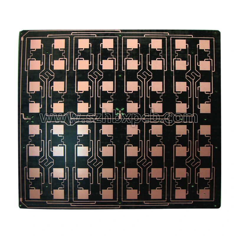
The manufacturer title says 5.8G dual polarisation. This is an application label, with no measured gain, cross-polarisation, bandwidth or radiation report.
Engineering response: Identify the exact F4BM supplier / grade and lot, stack tolerances, array / feed geometry and RF test fixture; agree which antenna-performance measurements are actually delivered.
The F4BM title includes “5.8G dual polarisation,” but its detail page contains no radiation pattern, gain, bandwidth, cross-polarisation or measured return-loss report. Specify the actual operating band and acceptance with feed geometry, substrate variation, launches and measurement fixture. An array photograph cannot determine these results.
Whole corresponding manufacturer catalogue photograph. Board dimensions and measured RF performance are not inferred from the image.
Arlon double-sided PCB reference
Published construction
Arlon — exact grade not supplied · 2 layers
Board thickness
1.6 mm
Copper / finish
1 oz / immersion gold
Mask / legend
Not stated on this specific reference
Arlon is the only material identity in this product record; the general introduction lists several families but does not select one for this board.
Engineering response: Name the exact laminate grade, dielectric test method, copper and traceability; do not accept a generic Arlon substitution without stack and RF review.
The company introduction lists several Arlon-related grades, whereas this product record only says Arlon. Choose the required grade from your electrical and mechanical design, then ask the factory to confirm procurement and processing. A brand-level substitute can change the stack and RF behaviour; it needs written engineering approval.
SPECIAL CONSTRUCTION / AN INNER FEED EXPOSED THROUGH THE FIRST DIELECTRIC
The Taconic / FR-28 stepped cavity needs a cross-section drawing.
Whole corresponding manufacturer catalogue photograph. Board dimensions and measured RF performance are not inferred from the image.
Taconic / FR-28 stepped-cavity reference
Published construction
Taconic grade unreported; FR-28 special prepreg · Layer count not supplied
Published construction
1.524 + 1.524 Taconic layers; units omitted in source
Bonding / opening
FR-28 special prepreg; first dielectric opened to expose inner feed
Metal finish
Immersion gold
The source describes a bonded cavity construction, not a finished thickness or layer count. The two 1.524 values have no explicit unit, so they are not added into a 3.048 mm finished-board claim.
Engineering response: Supply a section drawing with material / bond film identity, finished stack, cavity depth, exposed conductor and datums; agree bonding, planarity, registration and RF acceptance.
Stack and bond line
The official description gives “1.524 + 1.524” Taconic material and FR-28 special prepreg. It does not attach units, name the Taconic grade, specify the cured bond line or state finished layer count. Do not sum the two values into a finished thickness. Supply a controlled section with material, starting and finished dimensions.
Opening and feed interface
The first dielectric is opened to expose an inner feed; the metal is immersion gold. Dimension the cavity from datums, its depth and registration, the exposed conductor and clearance. Agree adhesive flow, planarity, surface finish and inspection at the opening, plus any RF coupon / fixture that represents this transition.
OFFICIAL PROCESS TABLE / THE HEADING IS “LIMIT CAPABILITY — SAMPLES”
Read copper, drill and impedance conditions together with the design.
The general process table is explicitly presented as sample-limit capability. It is useful for an engineering conversation, but is neither the specification of the nine pictured references nor a guarantee for series production. Its 1–32 layer and 0.1–20 mm ranges must not be combined with every minimum feature.
Finished-copper geometry
0.5 oz
3 / 3 mil line / space
1 oz
3 / 4 mil line / space
2 oz
5 / 6 mil line / space
These are different rows under finished copper. A 1 oz reference does not inherit the 0.5 oz spacing limit. Ask for the accepted geometry at your copper, stack and quantity.
Mechanical drilling
Minimum drill
0.15 mm only with board thickness below 1.2 mm
Aspect ratio
10:1; 12:1 only for diameter at least 0.35 mm
These are drill / aspect conditions, not a 0.15 mm finished plated hole. Release finished hole, tolerance, plating and stack; confirm the drilling route in the reply.
Impedance acceptance
Target at or below 50 Ω
±5 Ω in the general row
Target above 50 Ω
±10% in the general row
Separate limit row
±5% for targets at least 50 Ω
The rows overlap at 50 Ω. Agree which requirement applies, the stack and coupon, measurement method and yield expectation. An absolute ohm limit is not a percentage.
The table also names laser holes of 0.1–0.15 mm and a 0.9:1 dielectric / diameter condition, plus specific blind-via and multilamination structures. Those entries do not demonstrate an installed laser drill or establish that a PTFE / hybrid cavity design can use all the same limits. Request a stack-specific process response.
Some detailed finish and plugging rows contain units or ranges that need clarification. They are not converted into catalogue promises here. For immersion gold, OSP or other finish, state the required finish standard, thickness and inspection in the order drawing.
RF ACCEPTANCE / DEFINE THE TEST OBJECT BEFORE THE TEST LIMIT
A bare-board netlist result and an RF device measurement answer different questions.
Fabricated PCB
Specify material / lot trace, layer and finished dimensions, copper and finish, plated-hole integrity, electrical continuity / isolation and any coupons. Record the applicable IPC revision, class and customer drawing.
RF structure or assembled device
Define launches, fixtures, calibration reference planes, frequency sweep and S-parameter acceptance. Antenna radiation, amplifier gain / power and combiner isolation require their own test object and method.
The website’s impedance-matching article contains a 5.3–5.5 GHz amplifier example and simulated / measured results. It is technical article content, not a qualified performance sheet for the RF-35 catalogue PCB. The reviewed equipment captions also do not establish a calibrated VNA or TDR configuration.
Specify the actual finish and schedule
An older design-advice article discourages OSP, while multiple official products expressly specify OSP. Use the current agreed build, handling and assembly window for your order rather than treating the article as a universal prohibition.
The 2022 material-stock article says supplier material can arrive in 1–5 days when available. That is material procurement, not finished-board turnaround. Reserve fabrication time after stack approval and material confirmation, including outside operations, inspection and transport.
CAPTIONED PRODUCTION INVENTORY / IMAGING IS NOT DRILLING
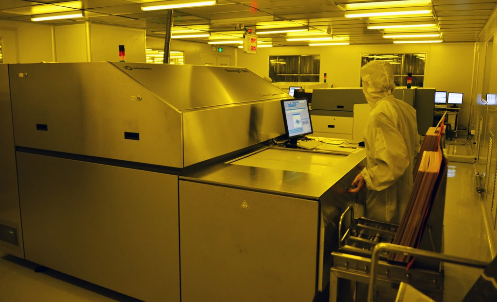
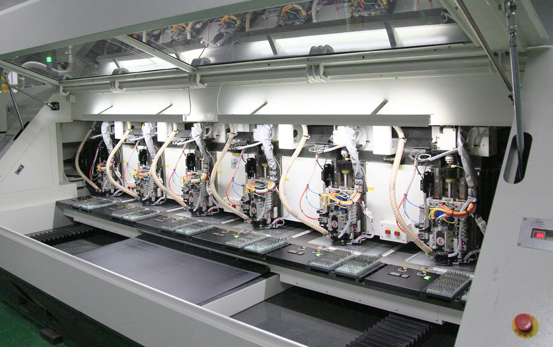
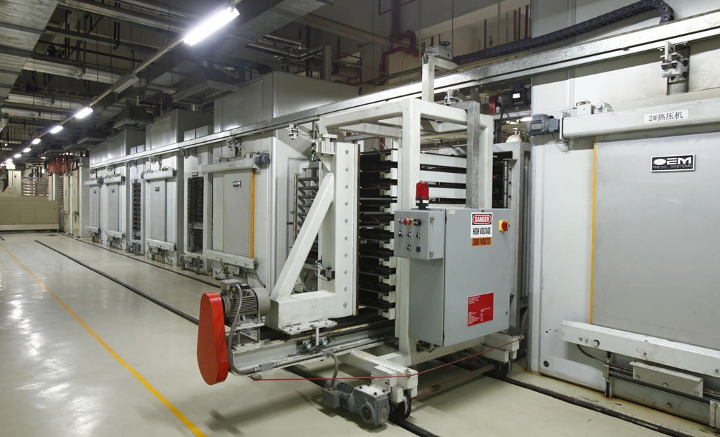
The equipment pages show LDI, mechanical drilling, AOI and lamination operations.
Official equipment image captioned LDI laser direct imaging. This is imaging, not evidence of laser drilling.
Expose and register
The manufacturer captions LDI, dry-film development / lamination and solder-mask exposure. Confirm layer registration, imaging compensation and mask keep-outs for the material and conductor pattern you release.
Official equipment image captioned high-speed six-axis drilling. No machine model, current serial or accepted hole limit is established by the photo.
Drill the actual stack
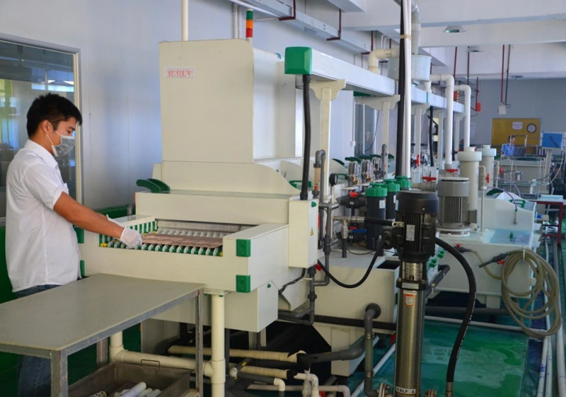
The mechanical-drill caption and sample table should be connected by a written route response. Ask about hole-wall preparation, plating, entry / backing and the acceptance of your laminate combination.
Manufacturer-captioned lamination equipment, whole original photograph.
Bond
Agree material-specific press conditions and the cavity / bond-line acceptance. A press photo does not establish a cured dielectric or bond result.
Manufacturer-captioned precision vacuum etching, whole original photograph.
Etch
Link compensation and inspection to finished copper and geometry. The table changes spacing with copper weight.
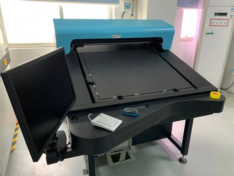
Manufacturer-captioned AOI, whole original photograph.
Inspect
Define optical inspection and repair criteria, then distinguish these from netlist electrical and RF measurement results.
Thirteen equipment captions were read across both pages, also covering oven, plating line, etching line and CNC. The review establishes what the manufacturer publishes; it does not establish a current machine register, calibrated RF-test inventory, outside-process boundary or an independently visited site.
CONTRACT, PRODUCING ADDRESS AND DOCUMENT SCOPE
Match the RF order to Shenzhen Huabangxin and the Fuyong disclosure.
Official contact identity
The company and contact pages name 深圳市华邦鑫电路科技有限公司, with Building 10, Lisheng Industrial Zone, Fuyong, Bao’an, Shenzhen (深圳市宝安区福永利昇工业区10栋). Contact Mr Li; telephone 18680060886; published email hbxpcb@vip.163.com.
This is the manufacturer’s current website disclosure, not an independently checked mailbox-control result or a site visit. Match the contractual entity, invoice and actual producing / outside-processing locations before releasing controlled manufacturing files.
Quality language versus order documents
The introduction describes ISO quality-management practice, IPC-A-600G Class 2 and RoHS conformity. The quality page separately refers to IPC-6018A and process-management methods. The reviewed pages do not establish a current certificate issuer / holder / validity record or a UL File Number.
Specify the revision, class, customer requirements and conformity evidence for the actual RF build. Historical standard references and management language do not replace a current order acceptance or material declaration.
The footer’s 2011–2022 copyright range is not a documented founding date. The introduction’s dielectric range of 2.2–10.2 and a 2022 article’s 2.2–10.6 wording are broad material statements; neither is a measured constant for every board shown here. Select the actual grade and its test basis.
RFQ RELEASE / DRAWING, TRACEABILITY AND MEASURED ACCEPTANCE
Ask for an engineering reply that resolves the chosen build.
Grade and procurement: full laminate and bond-film codes, manufacturer datasheet / revision, copper construction, lot trace and authorised substitutes.
Stack and geometry: dielectric and finished thickness, copper by layer, line / space, finished holes and plating, cavity section / datums if applicable.
Surface and interface: finish, mask / legend keep-outs, launches, pads, storage / assembly window and the supplied bare-board versus assembly boundary.
Acceptance and records: IPC revision / class and customer drawing, netlist / coupon tests, calibration and RF limits when contracted, inspection and trace records.
Route and schedule: producing entity / site, in-house and outside steps, material availability and finished-order lead time after engineering approval.
Reviewed 9 October 2026. Nine independently mapped catalogue references are selectable within this existing factory page. Unreported per-reference geometry stays unknown; the conditional sample table remains an engineering discussion rather than an automatic combination of extreme values.
Official company, contact, process and quality pages, both equipment pages and individual product details were read separately. Original product links and whole equipment images were mapped to their own records. Rogers material identity is supported by its original page; it does not endorse this factory or verify its purchases. Customer-logo decorations, educational RF results and conflicting article conversions are excluded from product qualifications.