HOPESEARCH / COPPER, EDGE AND CONTACT CONSTRUCTIONS
Compare the construction before comparing the quote.
Hopesearch’s Shenzhen company, 深圳市丰达兴线路板制造有限公司, dates its establishment to 2002. It describes high-density double-sided and multilayer PCB manufacture and the opening of a Pingxiang factory in late 2019. The official catalogue is especially useful for separating thick copper, plated half-holes, carbon contacts and mixed surface finishes. Those features create different fabrication and assembly requirements even when the layer count is modest.
The four examples below are taken from individual product-detail pages. They have their own thickness, finished-copper notation, paired line/space and mask-bridge entries. Keep each combination intact when shortlisting; the eight-layer thick-copper example cannot inherit the finer routing of the four-layer mixed-finish example.
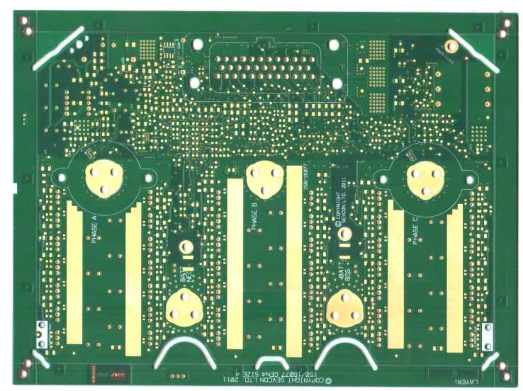
Original photograph from the eight-layer thick-copper entry. The application, dimensions and current rating are not inferred from the artwork or printed customer markings.
Construction
8 layers / 1.6 mm
Finished copper notation
3/3 oz
Line / space
0.15 / 0.15 mm
Mask bridge
0.15 mm
Finish / mask
Immersion gold / green
Minimum-hole entry
0.2 mm; definition to agree
The card explicitly calls the copper “finished copper”. Preserve the 3/3 oz notation and ask for its assignment to the complete eight-layer copper schedule. Do not assume every layer has the same thickness or substitute the general table’s base-copper maximum. The product’s 0.15/0.15 mm routing and 0.15 mm mask bridge belong to this example.
Supply continuous and transient currents, allowable temperature rise, terminal geometry and the intended thermal boundary conditions. Ask for the proposed copper by layer, plated-hole copper, laminate and the etched geometry used in the thermal assessment. The page gives no current rating, material grade or board dimensions. Its 0.2 mm hole entry must be clarified as drilled or finished before accepting a drill file.
TWO INTERFACE ROUTES / EDGE SOLDERING OR CARBON CONTACT
The interface determines the acceptance test.
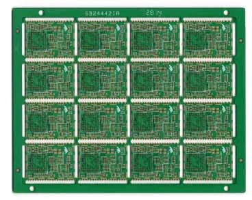
Four-layer immersion-gold half-hole board
Exact card 815847: four layers, 1.0 mm, green mask. Native-width image retained in full.
Finished copper
1/1 oz
Line / space
0.10 / 0.10 mm
Mask bridge
0.10 mm
Minimum-hole entry
0.2 mm
A half-hole module needs an edge drawing as well as a drill file. State the plated-hole centre relative to the final outline, remaining copper, edge burr limits, solderable area and allowable mask clearance. Ask which operations occur before and after routing and how the exposed plated edge is inspected. The catalogue label does not define an edge-pull strength or a dimensional tolerance.
Include the module’s assembly panel, handling rails and mating-board land pattern. Agree the finish specification and inspection of the soldering interface with the assembler. The published 1/1 oz notation and 0.10 mm routing do not supply an internal copper schedule or the accepted finished-hole diameter.
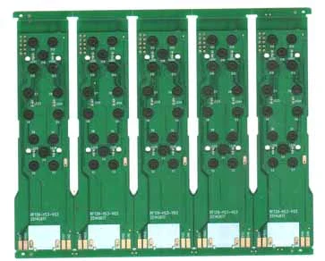
Double-sided immersion-gold and carbon board
Exact card 816153: 1.6 mm, green mask, immersion gold plus carbon ink. Native-width image retained.
Finished copper
1/1 oz
Line / space
0.15 / 0.15 mm
Mask bridge
0.10 mm
Minimum-hole entry
0.2 mm
For a carbon-contact circuit, release the carbon layer and its registration to the copper and mask. Specify the contact geometry, mating material, operating force, acceptable resistance and the expected wear or switching duty. The photo does not establish the carbon formulation, coating thickness, curing profile or contact life.
The card names both immersion gold and carbon ink. Identify their distinct zones and any required overlap or separation. Agree whether resistance is measured on a coupon, on the actual contact pair or after a defined wear sequence. A standard netlist electrical test alone does not express the contact behaviour the buyer needs.
FOUR-LAYER MIXED FINISH / CATALOGUE 815863
Gold, OSP and impedance belong on one released stack.
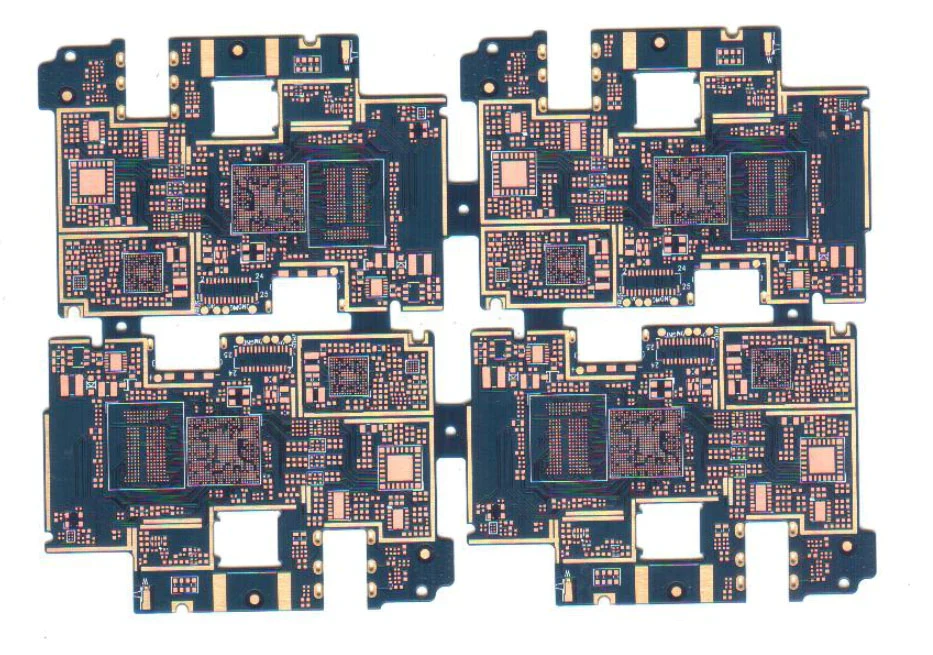
Original mixed-finish catalogue photo. The card specifies four layers, 1.0 mm, black mask, finished copper 1/1 oz, 0.075/0.075 mm line/space and a 0.10 mm mask bridge.
The title calls this an impedance board, but the product card gives no impedance target or tolerance. The current general process table lists ±10% in its 2026 column; that is a discussion point, not a measured result for this construction. Submit the single-ended and differential targets, reference planes and coupon requirements with the laminate and copper schedule.
Mark the immersion-gold and OSP zones, and agree the finish specification, packaging and assembly sequence. Define how the mixed finish is inspected and what changes require renewed approval. The 0.2 mm minimum-hole entry remains unspecified as drilled or finished. Obtain the proposed dielectric and return DFM before treating 0.075 mm routing as compatible with the entire drawing.
DATED PROCESS CHART / REVIEWED OCTOBER 2026
Keep sample, volume and future-year columns apart.
The current official chart has 2026 and 2027 headings. Within the 2026 column, it explicitly separates sample and volume layer/thickness values. The 2027 values are kept outside this profile’s current capability filters; the page does not explain their qualification or availability.
2026: sample and volume entries
Layers
Sample: 32 / volume: 16
Maximum thickness
Sample: 4.0 / volume: 3.2 mm
Minimum thickness
Sample: 0.3 / volume: 0.4 mm
Routed-outline tolerance
Sample: ±0.075 / volume: ±0.1 mm
2026: other chart entries
Base copper
Inner and outer: ⅓–6 oz
Inner / outer line-space pairs
0.075 / 0.075 mm in each entry
Minimum through-hole entry
0.15 mm
Impedance tolerance
±10%
PTH / NPTH diameter tolerance
±0.076 / ±0.05 mm
Shipped panel format
600 × 750 mm
The table also lists a 12:1 plated through-hole aspect ratio and 0.8:1 laser-hole ratio. These are different processes. Do not derive a finished-hole diameter by dividing the maximum thickness by the aspect ratio, or assume the minimum routing is available at 6 oz base copper. Ask for the complete proposed stack, drill/plate definition and copper-dependent routing rule. None of the chart maxima replaces the four illustrated constructions’ specific parameters.
The official contact page lists both mainland entities and a Hong Kong business address at Rooms 1318–19, Hollywood Commercial Centre, 610 Nathan Road, Mong Kok. Use the actual fabrication entity and site on the quotation. The reviewed product cards and group equipment gallery do not assign these four boards to a particular factory.
A separate original government record names the Shenzhen entity: the Shenzhen Industry and Information Technology Bureau’s notice of 11 October 2025 includes 深圳市丰达兴线路板制造有限公司 as entry 58 in the 2025 Shenzhen Green Factory list. This is a dated, city-level designation for that named entity. It is not a UL ownership check, automotive programme approval or certification of the Pingxiang operation.
Inspection route to request
The official equipment page lists vertical plating, pressing, drilling, DES/SES processing, dedicated and flying-probe electrical testers, an impedance tester, inner-layer X-ray, thermal shock and line-width measurement. Agree which line and instruments will be used at the chosen site, what calibration applies, and which results accompany the shipment. The gallery is a manufacturer disclosure, not a current site-by-site machine inventory.
For first-article release, request the approved stack/material/copper schedule, outline and interface inspection, electrical-test revision, impedance coupons where required and lot traceability. For repeat orders, define permitted substitutions and process/site changes. Start with the relevant example above and attach its specific edge, contact or finish requirements to the RFQ.
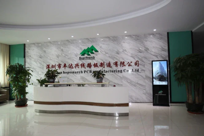
Individually researched on 8 October 2026. Four original product photos were matched to their exact detail pages and viewed in full, together with the current logo and two labelled factory reception photographs. The current sample/volume/year columns, equipment text, contact entities and original government notice were read separately. Finished-copper notation is retained without inventing a layer schedule; unspecified hole definitions remain for drawing review. City-level recognition and manufacturer process disclosures have distinct scopes.