

Eight layers, Tg170 FR-4 and one-ounce copper.
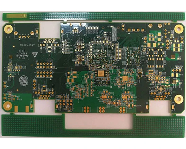
The entry specifies FR-4 Tg170 and a 0.20 mm minimum through-hole. It does not identify the laminate manufacturer or grade, and “through-hole” does not establish the finished plated diameter. Send the actual stackup, finished-hole schedule and impedance requirements; the photograph does not provide those design files.
This is a more specific starting point than the general rigid capability sheet’s independent maxima of 38 layers, 20 oz outer copper and 0.075 mm line/space. Those values describe separate process limits; they do not replace this board’s one-ounce, eight-layer construction.
Ten layers: 1 + 1 + 6 + 1 + 1.
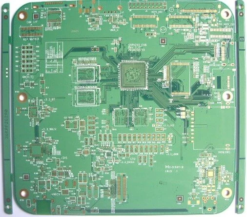
The industrial-control example identifies a six-layer core with two build-up layers on each side. Its published material is FR-4 Tg150, thickness 1.6 mm, copper 17.5 μm on all layers, green solder mask and immersion gold.
- Hole label
- 0.10 mm; via type and finished diameter need definition
- Impedance
- Control mentioned; target and tolerance are not supplied
- Routing row
- Literal “Trace width/width: 0.89/0.1mm”
The routing row cannot safely be corrected to 0.089 mm or interpreted as a minimum line/space pair. Ask engineering for the current drawing rules and which copper stage the values describe. Include microvia layer pairs, capture pads, dielectric thickness, via fill and the coupon acceptance requirements.
A separate product page is headed “24 layers” but follows with a broad 3–36-layer HDI table. This profile does not assign that generic table to the ten-layer photograph or present it as a tested 24-layer construction.
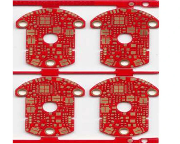
A compact six-layer board with three-ounce copper.
- Dimensions
- 70.8 × 76.2 mm
- Thickness / laminate
- 2.0 mm / FR-4 Tg150
- Inner and outer copper
- 3 oz, as stated for each
- Minimum through-hole
- 0.60 mm; finished definition not provided
- Finish / application
- Immersion gold / position-control systems
No line/space pair is supplied for this particular board. For a power redesign, specify current, temperature-rise allowance, copper-by-layer and thermal interfaces. Ask whether the three-ounce values refer to starting foil or finished copper, and agree the measurement locations.
Make the transfer between services explicit.
The assembly page offers full turnkey, partial turnkey and consigned components, plus coating and box-build. It also explicitly describes a network of PCB assembly and manufacturing partners. Agree the production route and approved outside processes before release; a one-stop quotation does not establish that every operation occurs at one Hitech-owned site.
Release a consistent data set.
Supply fabrication files, stackup, BOM, component positions, assembly drawings and revision identifiers. Define sourcing authorisation, approved substitutions and the documents required for traceability.
Specify what the test proves.
The PCBA page lists AOI, ICT, FCT, burn-in and other test options. Its functional-test description calls for customer-defined fixtures, test points, program and procedure. Set limits, coverage, sampling and the report to be delivered; availability is not automatic inclusion.
Agree site and shipment gates.
Confirm the assembly location and acceptance authority. Published estimates of 1–3 days for prototype assembly and 4–10 for medium batches are not a complete procurement schedule. Agree when the clock starts after components and engineering data are ready.
The general table lists mechanical finished-hole minimum 0.15 mm, laser finished-hole minimum 0.10 mm and ±10% impedance. Those separate process rows do not qualify a specific HDI or assembled design. The quality page’s yield, complaints and delivery percentages are stated goals, not audited results adopted by this profile. Its equipment gallery does not provide a model-by-model inventory.
Build a complete engineering brief →Choose substrate and metallisation together.
Beyond the three FR-4 examples, Hitech publishes metal-core, flexible, rigid-flex and ceramic services. Ceramic descriptions mix thin/thick-film metallisation and direct-bonded copper. Request the selected substrate grade, metallisation route, copper thickness and joining process rather than treating “ceramic PCB” as one interchangeable construction.
The ceramic capability’s 50/50 μm routing statement is conditioned on base copper below 10 μm. It cannot be carried into its separate 18/35/70 μm copper rows. Thermal-conductivity ranges differ between the capability table and product discussion without matching test conditions. Ask for the material supplier’s data sheet and lot documentation; no generic temperature or conductivity value is assigned to a pictured board.
Flexible layer-count statements also differ: the company overview lists up to 16, while the capability table lists 1–12. A rigid-flex order needs separate rigid and flexible stack details, bend requirements and engineering approval.
Define the material evidence required →The assembly scope and the UL holder answer different questions.
The official contact page names Hitech Circuits Co., Limited at 2F, Building C, Suojia Technology Park, Hangcheng, Bao’an, Shenzhen, Guangdong 518126. The company overview also describes Shenzhen and Meizhou operations; those descriptions do not identify which site will make a particular order. Both sales@hitechcircuits.com and sales@hitechpcb.com appear on the current contact page.
UL file E354070: holder cross-check.
UL’s public Trade Names list names HITECH CIRCUITS CO LTD against E354070. The manufacturer-hosted model sheet names HT-AL1, HT-M and HT-D but prints a last-update date of 14 December 2020. Its 2026 upload path is not a current model-scope confirmation. Obtain the current applicable construction and marking requirements for the ordered board.
IATF copy: PCBA at the Shenzhen address.
The hosted certificate names Hitech Circuits Co., Limited and the Suojia address, with scope “Manufacturing of Printed Circuit Board Assembly (PCBA)” and product design excluded. It lists IATF 0612421, CATARC 2026CAC0165, USI GZCTNA and dates 21 August 2026–20 August 2029. This review read the manufacturer-hosted copy, not a live issuer confirmation. The stated scope is not blanket certification of bare-board fabrication or every branch site.
For an automotive assembly RFQ, put the legal quote entity, production address, certificate scope, design responsibility and required customer approvals into the release checklist. For bare boards, separately define UL construction, laminate traceability and electrical-test documentation.
Sources behind this profile
Individually researched on 8 October 2026. Three photos are tied to their own product entries. Source ambiguities are kept beside the affected design decision; certificate copies and the independent UL holder list have different evidential scopes.
- MANUFACTURER / COMPANYBusiness and branch descriptions ↗
- MANUFACTURER / RULESRigid, flexible, metal-core, ceramic and assembly capability ↗
- MANUFACTURER / EIGHT LAYERSEight-layer parameters and original photograph ↗
- MANUFACTURER / TEN-LAYER HDI1+1+6+1+1 entry and routing wording ↗
- MANUFACTURER / POWERSix-layer three-ounce board ↗
- MANUFACTURER / HDI SCOPE24-layer heading and generic process table ↗
- MANUFACTURER / CERAMICCeramic service and process discussion ↗
- MANUFACTURER / ASSEMBLYAssembly services and partner-network description ↗
- MANUFACTURER / TESTINGCustomer-defined functional testing and test options ↗
- MANUFACTURER / QUALITYQuality goals and equipment gallery ↗
- MANUFACTURER / CERTIFICATE COPIESHosted IATF and dated UL images ↗
- UL / PRIMARY HOLDER LISTTrade Names list: HITECH CIRCUITS CO LTD / E354070 ↗
- MANUFACTURER / CONTACTShenzhen address and both service-email domains ↗