H-FAST / HEHONG · PCB, SPECIAL CONSTRUCTIONS AND PCBA
Start with the deliverable: a power board, a thermal construction or a tested assembly.
Hehong’s official catalogue is unusually broad: conventional multilayers sit beside thick copper, embedded polymer materials, aluminium, ceramic, high-frequency circuitry and PCBA. The Shanghai company and the Jiangsu producing entity share the H-fast brand. For a buyer, the first useful decision is which construction will be fabricated, at which site, and where bare-board responsibility ends and assembly responsibility begins.
Thirty-five individual product details were read for this review. Ten references below retain their own original pictures and published identities. The large copper weights and application labels are useful starting points; they do not replace a stack drawing, measured test limits or written acceptance of the combined design.
POWER BOARDS / CURRENT, COPPER AND INSULATION HAVE DIFFERENT ACCEPTANCE CRITERIA
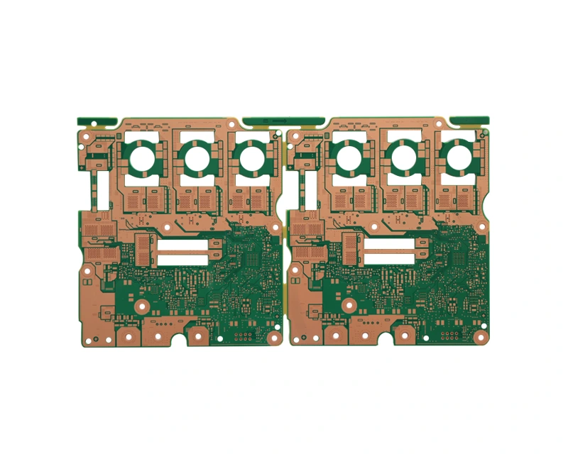
Keep 48 V DC–DC, 4 oz / twelve layers and 9 oz as three separate references.
Whole corresponding official catalogue image. Photograph scale, colour and filename are not specifications.
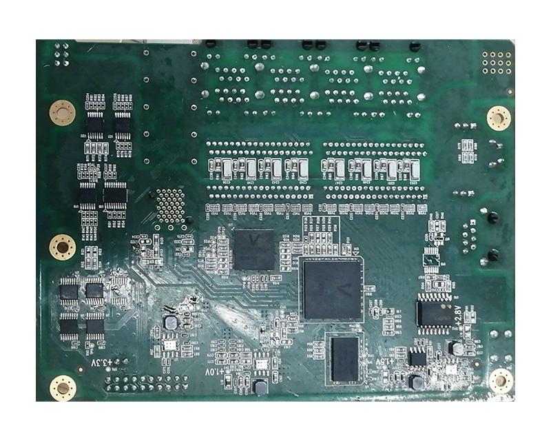
Multilayer PCB reference for 48 V DC–DC
Published reference
The official title identifies a multilayer automotive board for 48 V DC–DC. It does not state layer count, copper, material, insulation, current or operating temperature.
Drawing-specific geometry
Trace / space, finished hole and impedance are not stated
Order acceptance
Release the power-stage stack, current and thermal conditions, copper by layer, creepage / clearance, isolation and test acceptance. Require the producing site and automotive qualification scope for the actual order.
Electrical duty
A 48 V application title is not a rated current, working-voltage insulation result or conversion efficiency. Specify nominal and transient voltage, conductor current, allowed temperature rise, creepage / clearance, isolation and the relevant inspection limits. Establish whether Hehong supplies only the PCB or also the populated and tested converter.
Production stack
Provide the copper and dielectric requirement for each layer, material grade, finished thickness, plated holes and mechanical interface. Ask the factory to accept the stack and geometry together; the other thick-copper pictures do not define this DC–DC board.
Whole corresponding official catalogue image. Photograph scale, colour and filename are not specifications.
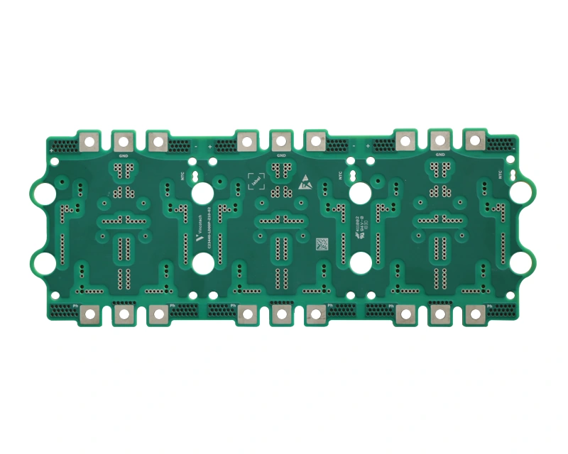
12-layer / 4 oz copper reference
Published reference
4OZ-12层板 explicitly names twelve layers and 4 oz. The page repeats this title without a layer-by-layer stack or base-versus-finished copper definition.
Drawing-specific geometry
Trace / space, finished hole and impedance are not stated
Order acceptance
Define the copper requirement for each layer, laminate, lamination, finished holes, geometry and thickness. Agree etch compensation, plating and microsection acceptance for the combined design.
Whole corresponding official catalogue image. Photograph scale, colour and filename are not specifications.
9 oz thick-copper board reference
Published reference
9OZ厚铜板 names 9 oz thick copper, without layer count, copper placement or base-versus-finished scope. It is a separate example from the 12-layer / 4 oz board.
Drawing-specific geometry
Trace / space, finished hole and impedance are not stated
Order acceptance
Provide conductor cross-sections, finished copper by layer, current / temperature-rise criteria, etch compensation, dielectric spacing and plating acceptance. Do not infer current rating from the copper label.
The 4 oz page names twelve layers but otherwise repeats its title. The 9 oz page does not give a layer count. Neither identifies starting versus finished copper, inner versus outer layer distribution, minimum spacing at that copper weight or a current rating. Request etch compensation, plated-hole and microsection criteria, insulation distance and finished dimensions for the actual revision. Do not combine these titles into “12-layer / 9 oz / 48 V automotive qualified.”
MODULE EDGES AND EMBEDDED MATERIAL / DEFINE THE INTERFACE THAT WILL BE MEASURED
Castellated edges need a land-pattern drawing; embedded resistance needs an electrical specification.
Whole corresponding official catalogue image. Photograph scale, colour and filename are not specifications.
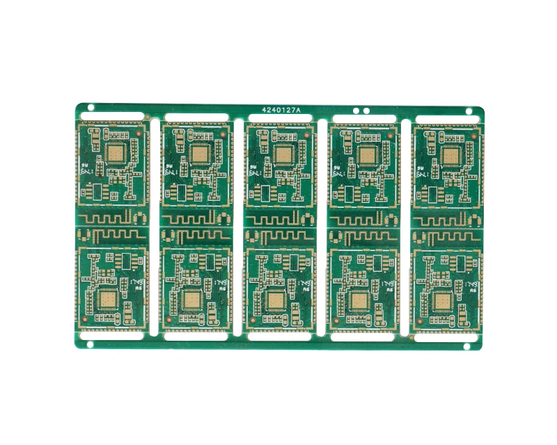
Multilayer castellated module reference
Published reference
多层半孔板(互联网模块) identifies a multilayer half-hole module board. Hole size, edge pitch, plating and dimensional tolerances are not published.
Drawing-specific geometry
Trace / space, finished hole and impedance are not stated
Order acceptance
Give the edge-pad / half-hole drawing, plated barrel acceptance, routed edge quality and motherboard land pattern. Clarify module assembly versus bare PCB scope.
For a half-hole module, dimension the pad pitch, finished plated barrels, routed edge and solderable surfaces against the host PCB land pattern. Agree the acceptable edge breakout and plating condition, how the outline is produced, and how alignment will be inspected. A module picture does not establish that the vendor supplies the module’s firmware, radio approvals or assembled function.
Whole corresponding official catalogue image. Photograph scale, colour and filename are not specifications.
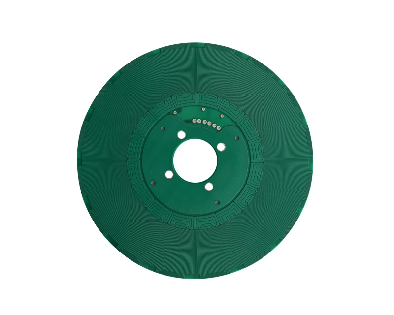
埋容、埋阻高分子材料 describes embedded capacitance and resistance polymer material. No electrical values, layer stack, process tolerances or reliability results are supplied.
Drawing-specific geometry
Trace / space, finished hole and impedance are not stated
Order acceptance
Identify the material grade, resistance / capacitance values and tolerances, location, test structures, measurement method and environmental qualification for the intended stack.
The embedded-material reference names both capacitance and resistance, but publishes no value, tolerance or temperature coefficient. Ask which of those functions is actually offered for your stack. Release the material and location, resistance / capacitance target, measurement structures and conditions, trimming if applicable, and drift / environmental acceptance. The research page’s polymer embedded-resistor work is not a result for this catalogue sample.
THERMAL CONSTRUCTION / THREE DIFFERENT PATHS FROM CIRCUIT TO HOUSING
Aluminium base, a ceramic substrate and a ceramic insert are not interchangeable.
ALUMINIUM BASE
Confirm dielectric insulation and thermal properties, circuit copper, base alloy / thickness and flatness. The contact to the housing is part of the thermal system.
CERAMIC SUBSTRATE
Identify ceramic composition, bonding / metallisation route and copper / ceramic thickness. Define soldering and handling limits, not just a conductivity number.
CERAMIC INSERT
Dimension the insert, cavity and bonded interface. Agree insulation, planarity and thermal cycling across the junction between materials.
Whole corresponding official catalogue image. Photograph scale, colour and filename are not specifications.
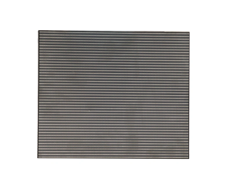
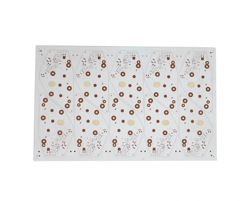
Single-sided aluminium-base reference
Published reference
单面铝基板 explicitly identifies single-sided circuitry on aluminium base. Dielectric, conductivity, isolation and base alloy / thickness are unreported.
Drawing-specific geometry
Trace / space, finished hole and impedance are not stated
Order acceptance
Specify the dielectric thermal and electrical requirements, circuit copper, aluminium alloy / thickness, flatness and mounting interface. Separate bare-board supply from a populated lighting assembly.
Whole corresponding official catalogue image. Photograph scale, colour and filename are not specifications.
Single-sided ceramic-circuit reference
Published reference
单面陶瓷板 identifies single-sided ceramic circuitry. It does not identify alumina versus aluminium nitride, DBC versus another bonding route, or substrate / copper thickness.
Drawing-specific geometry
Trace / space, finished hole and impedance are not stated
Order acceptance
State the ceramic composition, metallisation / bonding route, copper and substrate thickness, dielectric and thermal acceptance, soldering requirements and mechanical handling limits.
Whole corresponding official catalogue image. Photograph scale, colour and filename are not specifications.
Embedded ceramic board reference
Published reference
镶嵌陶瓷板 identifies an embedded-ceramic construction. Insert material, interface, stack, insulation and thermal results are not published.
Drawing-specific geometry
Trace / space, finished hole and impedance are not stated
Order acceptance
Release the insert and cavity drawings, interface / bonding requirements, electrical isolation, planarity and thermal-cycle acceptance. Keep the ceramic insert distinct from a complete ceramic substrate.
The research page discusses DBC ceramic-circuit technology, but the selected single-sided ceramic title does not identify DBC or the substrate composition. It cannot be labelled AlN, alumina, DPC or a particular thermal rating from the green solder mask or photograph. Likewise, the embedded-ceramic picture is not proof of a complete ceramic board stack. Specify the required construction and request a corresponding process and inspection response.
PCB TO PCBA / FABRICATION ACCEPTANCE IS NOT FUNCTIONAL ACCEPTANCE
One-stop supply needs an explicit division of responsibility.
Whole corresponding official catalogue image. Photograph scale, colour and filename are not specifications.
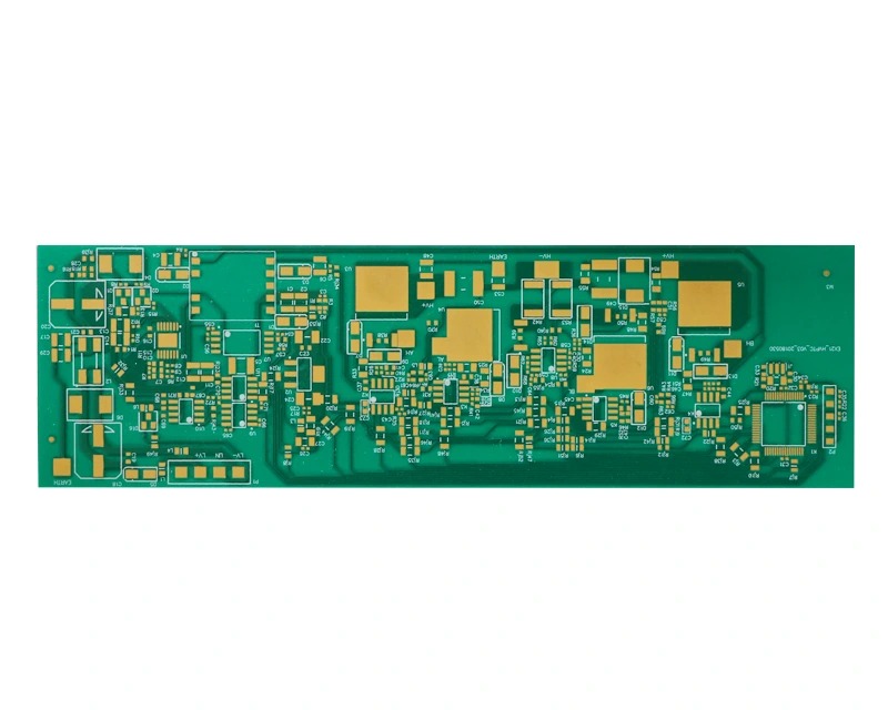
Industrial-control PCBA reference
Published reference
The PCBA category and 工业控制板 title identify an industrial-control assembly reference. Components, firmware, functionality and acceptance are not specified.
Drawing-specific geometry
Trace / space, finished hole and impedance are not stated
Order acceptance
Provide the BOM with approved alternatives, placement, fabrication and assembly revisions, component sourcing scope, programming and functional-test fixtures / limits.
01 / SOURCE
Release the controlled BOM, manufacturer part numbers and approved substitutions. Define who procures components, handles shortages, proves provenance and accepts customer-supplied material.
02 / BUILD
Link the bare-board drawing and netlist to placement and assembly revisions. Specify soldering, inspection, cleaning, rework and any special component / process conditions.
03 / TEST
Supply the programming image, version and functional-test fixture / method. Agree test limits, coverage, record retention, trace identifiers and packing. A populated board photo cannot provide these.
The official introduction offers PCB / PCBA manufacturing and turnkey material supply. It describes ten planned automotive SMT lines, with two installed at the time of that undated copy. This is not a current available-slot count. The PCBA gallery also contains automotive lighting references; an application label does not establish approval by an automotive customer or qualification of a complete lamp.
HIGH-FREQUENCY CIRCUIT / NAME THE LAMINATE AND MEASUREMENT METHOD
“Teflon high-frequency” supplies a material family, not a loss or impedance guarantee.
Whole corresponding official catalogue image. Photograph scale, colour and filename are not specifications.
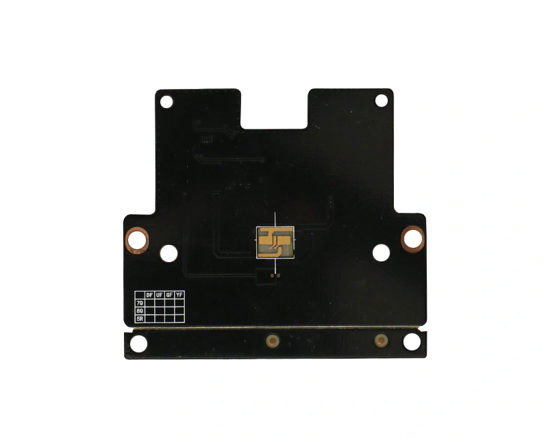
Fluoropolymer high-frequency board reference
Published reference
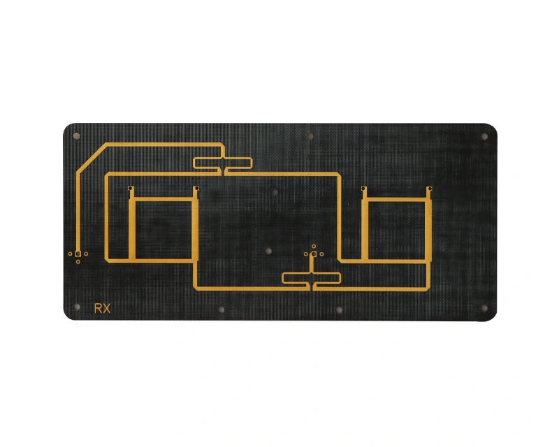
铁氟龙高频板 names a Teflon / fluoropolymer high-frequency board. No laminate brand, grade, frequency, loss or impedance tolerance is supplied.
Drawing-specific geometry
Trace / space, finished hole and impedance are not stated
Order acceptance
Define frequency band, laminate grade / properties, copper treatment, stack, impedance and loss criteria, calibration and coupon or network-analyser test method.
Agree the operating frequency, exact laminate grade, dielectric properties and tolerance, copper treatment, stack and launch / via design. Define which coupons or fixtures will be measured, calibration and acceptance for loss or controlled impedance. The manufacturer’s equipment collage labels a network analyser, but gives no configured frequency range or order report.
Another instrument is captioned as an impedance tester; the photographed instrument appears to be an LCR-style measurement unit. That caption alone does not establish time-domain PCB trace measurement. Request the actual method, fixture / coupon and calibration record before treating it as a TDR-controlled-impedance capability.
MANUFACTURER-CAPTIONED EQUIPMENT / CONNECT THE ROUTE TO AN ORDER RECORD
The original equipment sheets disclose operations; ask which are used for your stack.
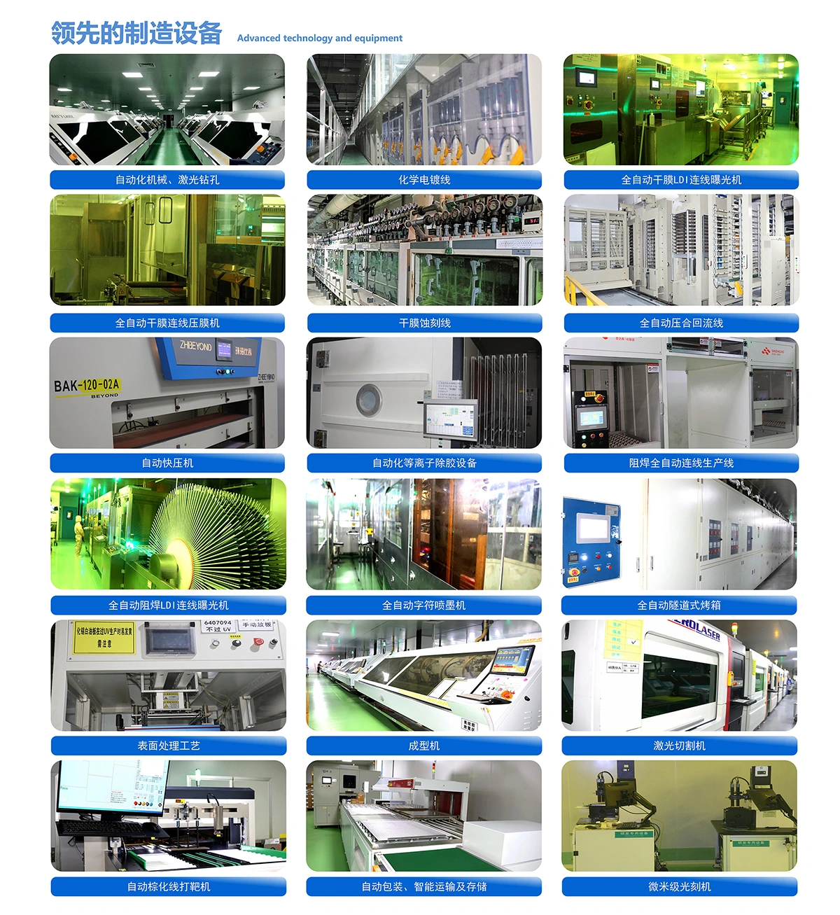
Whole official manufacturing-equipment sheet: manufacturer-captioned operations, not an independently audited asset list.
Manufacturing operations named by Hehong
The sheet explicitly names mechanical and laser drilling, dry-film LDI imaging, automated film lamination and etching, vacuum lamination, quick pressing, plasma desmear, solder-mask LDI, inkjet legend, surface treatment, forming and laser cutting. It also shows registration punching, packing / transport and laser marking.
Those labels are meaningful evidence of what the manufacturer presents. They provide no current serial register, machine count, acceptance window or commitment that a particular operation occurs at the Dongtai site for your revision. Define the route, site and any outside steps in the engineering response.
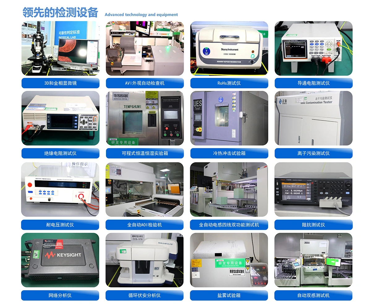
Whole official inspection / laboratory sheet. Instrument photographs and captions do not constitute a shipment test report.
Inspection outputs named separately
The test sheet labels microscopy, AOI and AVI, continuity and insulation resistance, withstand voltage, ionic contamination, temperature / humidity, thermal shock, salt spray, X-ray fluorescence screening, inductance / impedance instrumentation, network analysis and CVS bath analysis.
Choose the outputs your order actually needs: netlist electrical result, microsection, dimensions, finish / cleanliness, reliability or RF report. Agree specimen, method, calibration, sampling and limits. XRF screening is not by itself a complete RoHS declaration, and bath analysis is not a finished-board reliability result.
Match the contract and lot release to the correct Hehong entity.
Shanghai
The Chinese website names 上海贺鸿电子科技股份有限公司 and gives Room 402, Building E1, No. 1588 Zhuguang Road, Qingpu, Shanghai, telephone 021-33656999. Its company description places headquarters at Hongqiao World Centre.
The linked English site still gives No. 6280 Huancheng East Road, Zhelin, Fengxian, Shanghai. These are different office / entity disclosures, not two confirmed manufacturing sites. Confirm the current legal, contracting and correspondence addresses before issuing the purchase order.
Dongtai, Jiangsu
The manufacturer names 江苏贺鸿电子有限公司 at No. 8 Hongda Road, High-tech District, Dongtai, Jiangsu. General line 0515-85333888; business contact 0515-85390112. It publishes mkt@h-fast.com and mkt23@h-fast.com; mailbox control has not been tested.
The Chinese introduction describes phase-one premises of over 22,000 m² and a phase-two area of 21,000 m², with undated stated PCB capacity of 60,000 and later 100,000 m² per month. These are manufacturer descriptions of expansion, not independently measured output or currently available capacity.
Official architectural rendering of the proposed / described Dongtai campus. This is not a current aerial photograph or site inspection.
A government record tied to the exact producing address
Dongtai’s 5 December 2024 environmental-report publication names 江苏贺鸿电子有限公司, the heating-system upgrade project and No. 8 Hongda Road. It supports the entity / address match; publication alone is not approval.
The separate notice published 24 March 2025 lists the approval opinion for that project in row 3, 盐环东表复〔2025〕28号, issued 18 March 2025. This is a specific heating-system project decision. It is not blanket environmental compliance, a PCB quality certification or an independent factory audit by PCBVerified.
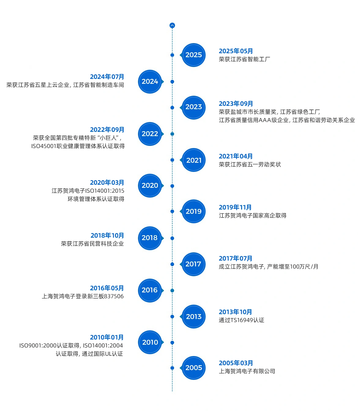
The manufacturer’s history dates the Shanghai business to March 2005, its NEEQ listing to May 2016 and the Jiangsu entity’s establishment to July 2017. The website displays code 837506. The original annual-report download was access-restricted during this review, so no current issuer financial or ownership claim is taken from search excerpts.
DATED HISTORY AND QUALIFICATION IMAGES / SCOPE BEFORE BADGES
Read the holder and period without extending a certificate to every board.
Management systems and historical claims
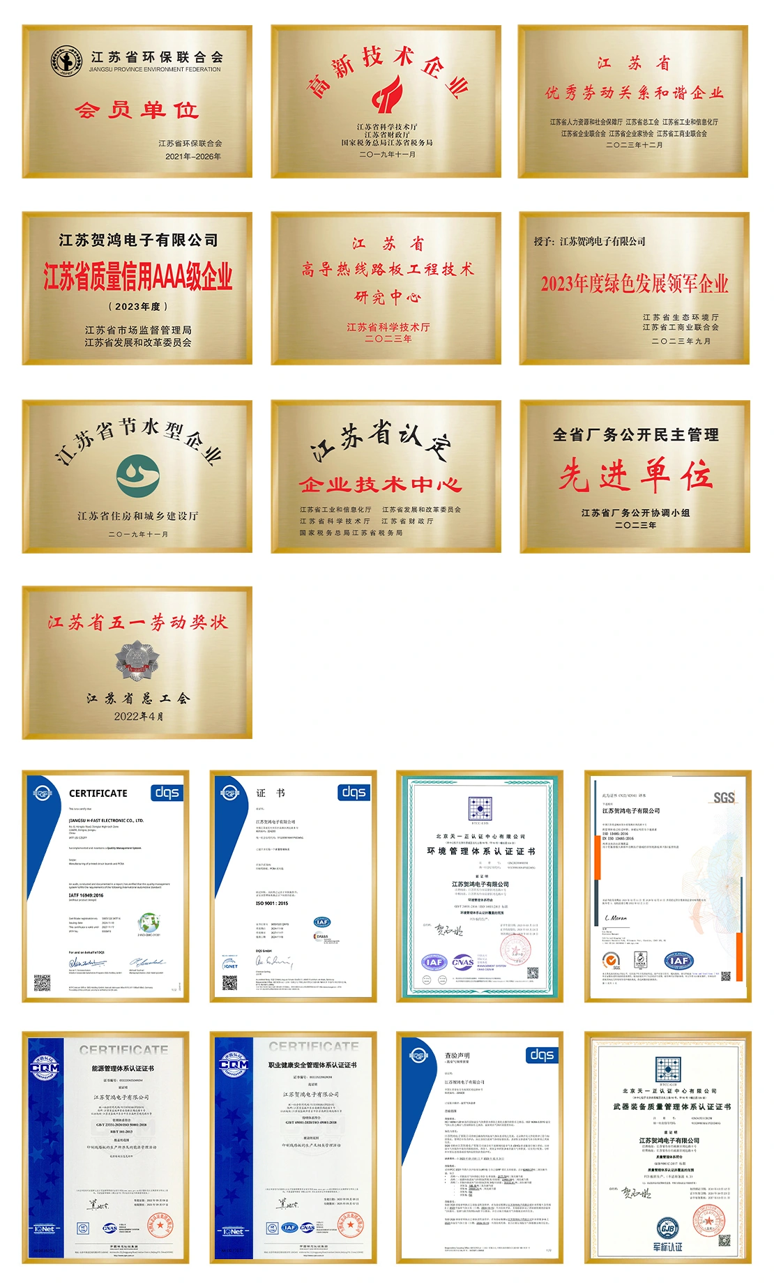
The honours collage contains Jiangsu H-fast / 江苏贺鸿 electronic-company management-system copies, including a readable IATF 16949:2016 heading and manufacture-of-boards / PCBA scope on the DQS image. Small serial, validity and annex text cannot be read reliably enough to establish current issuer status. The original is available below; request a legible current certificate and site / scope annex for the required contract.
The history image records a 2010 UL milestone and older ISO / TS milestones. It supplies no current UL File Number or board construction record. Sector names such as automotive, medical and radar are applications, not product approvals.
View the original honours / certificate collageWhole manufacturer-hosted honours / certificate collage. Low-resolution period and serial text is not represented as verified current status.
Patent and technology disclosures
The research page says 79 patent applications, comprising 38 invention and 41 utility-model applications. Applications are not a granted, live patent portfolio. It discusses DBC ceramic, polymer embedded resistance and RTR continuous plating as research activities; that does not assign those processes to every catalogue board.
Fengxian’s 23 July 2026 public notice lists 上海贺鸿电子科技股份有限公司 as item 13 under the 2024 patent-pilot enterprise reassessment group. It was a proposed acceptance list with a 23–29 July comment period. The reviewed notice is not the final decision or a test of PCB manufacturing quality.
View the original manufacturer historyManufacturer history through 2025. Historical milestones and different certification dates are not current issuer verification.
ENGINEERING RESPONSE / RELEASE THE BUILD, RESPONSIBILITY AND RECORDS TOGETHER
Request one written response for the exact Hehong order.
Construction and revision: identify the selected reference, drawing / netlist, stack, laminate or thermal material, copper by layer, finished holes, geometry and surface finish.
Interface and acceptance: define power / insulation, castellated edge, embedded electrical values, thermal bonding, RF method or assembly function as applicable. Use measured limits rather than application names.
Site and commercial scope: name the contracting entity, producing site, supplied materials and external steps. Resolve the Shanghai Chinese / English address difference.
Delivery evidence: agree lot trace, inspection and test records, qualification documents when required, programming / assembly responsibility and packing.
Schedule and change control: confirm an available production slot and authorised material / process substitutions. Undated expansion figures do not reserve capacity.
Reviewed 9 October 2026. Ten separately mapped references are selectable on this existing factory page; unknown drawing-specific measurements remain unknown. No customer-logo gallery is used as proof of approval or endorsement.
Thirty-five product details, corresponding original images, captioned production and test sheets, both official language disclosures and three government originals were reviewed independently. Animated counts, English placeholder text, inaccessible annual-report / green-factory files and customer-logo decorations are excluded from factual qualification claims.