Manufacturing site 1 · Fuqing
Fuqiang Industrial Park, Qinghua Road. The posted BSI quality-system copies name Fujian Fuqiang at this location.


MANUFACTURER DOSSIER
福建福强精密印制线路板有限公司 · Fujian
Fujian Fuqiang Delicate Circuit Plate Co., Ltd. (福建福强精密印制线路板有限公司) manufactures PCBs at Fuqiang Industrial Park on Qinghua Road, Rongqiao Economic Development Zone, Fuqing, Fujian. Its English website uses this company name and dates the business to 1996. The Chinese contact page also lists a second manufacturer, Fuzhou Ruihua Printed Circuit Board Co., Ltd. (福州瑞华印制线路板有限公司), at No. 37 Xiazhai, Guangming Village, Jingxi Town, Minhou County, Fuzhou.
Fuqiang Industrial Park, Qinghua Road. The posted BSI quality-system copies name Fujian Fuqiang at this location.
Ruihua at Xiazhai, Guangming Village. A shared sales contact does not transfer Fuqiang's certificate or catalogue parameters to this separate entity.
The public product catalogue includes a six-layer HDI construction, optical-module boards, heavy-copper power boards and ceramic-labelled high-frequency work. The technical page distinguishes standard and limit columns. Use those two levels to start a process discussion, then tie the selected construction, material and inspections to the actual supplying site.
A 12 September 2025 notice from the Fuzhou Industry and Information Technology Bureau lists Fujian Fuqiang in Fuqing among five proposed municipal industrial-design centres. This is a dated proposed-recognition notice; it is not a final approval, a product qualification or an independent factory audit.
These are separate entries in a general capability table, not one demonstrated board combining thirty layers, the finest conductors and the tightest impedance tolerance. The mechanical and laser fields do not state finished plated-hole sizes. The board-thickness bounds are the table's minimum and maximum rows, not a promise that every thickness/layer combination is available.
The HDI section lists stacked laser vias, blind-via filling, buried-via plugging and 2+N+2 as the maximum blind-via build-up in both columns. Ask for the actual via connections, copper stack and filling/planarization requirements. The general table also lists inner base copper of 0.5–12 oz and outer base copper of 0.5–14 oz, which should not be combined with the conductor minima specified at 0.5 oz.
The material row lists FR-4 Tg thresholds of 130, 150 and 170°C, halogen-free and CAF-resistant materials, plus ceramic, aluminium, Rogers-based, Teflon-based and high-speed materials. It does not identify a complete approved-grade list. Its CTI entry uses an unusual temperature unit; obtain the material datasheet and an unambiguous CTI requirement instead of treating that typography as a validated threshold.
Read how to compare combined limits →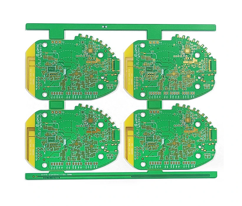
The page identifies through holes from layers 1–6, 0.10 mm blind holes from 1–2 and 5–6, and 0.20 mm buried holes from 2–5. It does not identify those diameters as finished plated holes. They stay in the construction notes, while the directory's finished-hole field remains unknown.
Provide the via table and fabrication drawing alongside the stack. Agree hole copper, filled-via condition, microsection locations and acceptance criteria. The named six-layer construction is distinct from the technical page's 2+N+2 maximum; do not upgrade the photographed example to that general maximum.
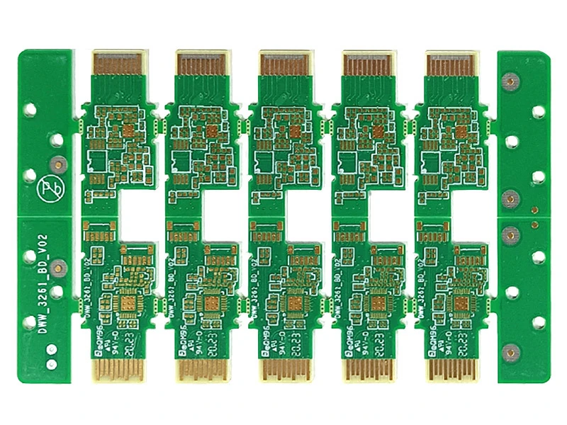
The source specifies Tg ≥170°C and TU-933, ENIG plus gold fingers, outline tolerance ±0.10 mm with local ±0.05 mm, and 95 Ω ±7%. It names server and data-centre optical-module applications, with laser and mechanical drilling, but does not publish a layer count or conductor pair.
Mark the nets to which the impedance target applies and confirm its mode, stack, coupon and reporting method. Define which outline features need the local tolerance, the contact geometry and gold requirements. Application wording alone supplies no data-rate or insertion-loss result.
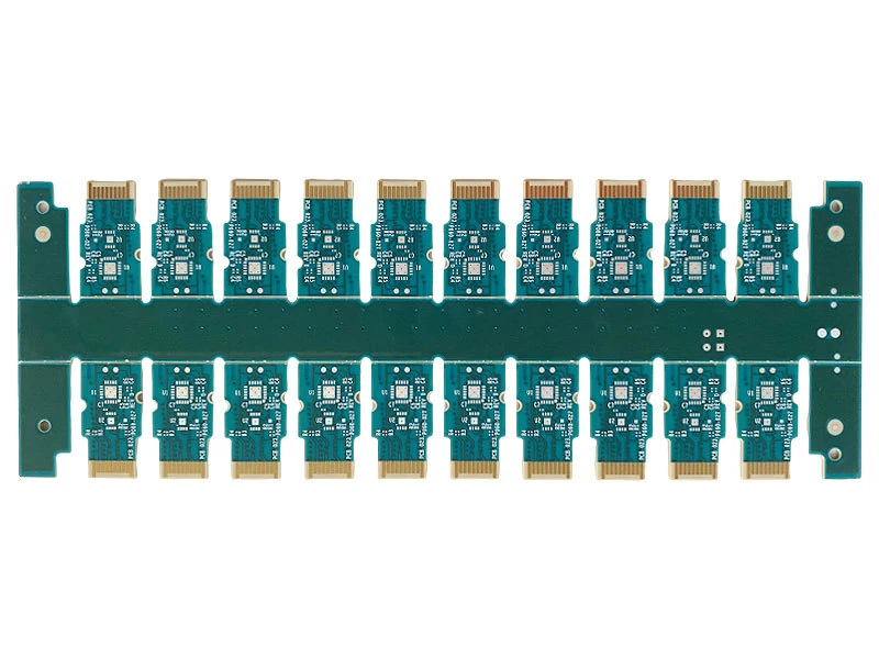
This separate page specifies six layers and immersion silver plus gold fingers, for high-speed 5G/optical-module use. The material grade and impedance target are not supplied. Neither TU-933 nor the other entry's ±7% tolerance is carried across.
Release finish zones, edge-contact dimensions and bevel requirements, along with storage and assembly conditions for the silver-finished pads. Obtain a stack and signal-integrity acceptance proposal for the actual module design.
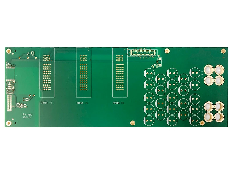
The manufacturer publishes 4.5 mm board thickness and copper as six ×105 µm and four ×500 µm. The same line prints a total as “2630 OZ”, which is inconsistent with the units of its layer entries. The layer figures are retained, but that printed total is not converted into an ounce rating or used as an order specification.
Request the copper thickness on each numbered layer, including starting versus finished copper and tolerance. Agree conductor geometry, resin fill, dielectric separation, drilling/plating and microsection acceptance as one stack review. The stated power-board use gives no operating current, thermal rating or load test.
The 4.5 mm example lies at the general table's published thickness limit. That does not mean it also meets the minimum 2.5 mil conductor pair or the maximum layer count. Ask for the process window for this copper distribution and your released geometry.
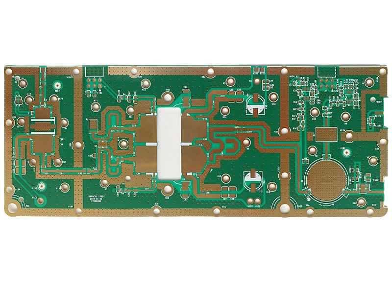
Detail 50 explicitly gives two layers and ENIG, for high-frequency reception and 5G products. The image does not identify its substrate chemistry. Request the actual ceramic material, metallization and stack, and the RF measurement requirements; no dielectric value or working band is published.
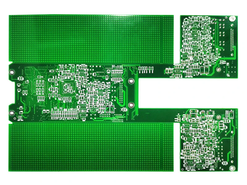
Detail 28 names this panel process but publishes no dimensional values. Supply the score start/stop locations, remaining web, panel support and depanelization requirements. Layer count and machining tolerances are not inferred from the photograph.
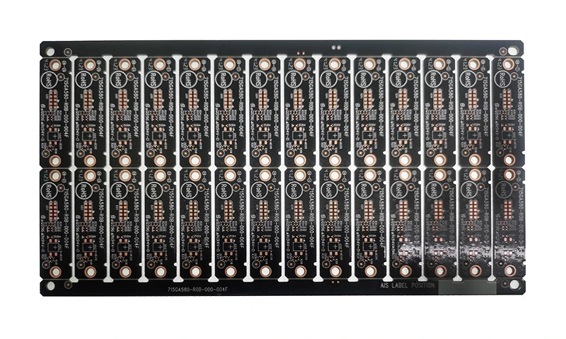
Detail 41 identifies a double-sided board, anti-oxidation surface treatment and black ink for consumer electronics. Confirm the precise finish chemistry, solder-mask requirements and assembly/storage conditions. The layer count follows the named double-sided construction, not a photographic inference.
The two-page production gallery names lamination, drilling, VCP and plating lines, LDI, vacuum etching, OSP, ENIG, solder levelling, routing and AVI. Three testing pages name impedance testing including a Polar system, microsection and hole-quality measurement, solderability, Tg, ionic contamination, metal thickness, four-wire testing, thermal cycling and a flying-probe room. These are manufacturer-labelled operations; models, counts and line allocation are not invented.
For model 1072, request via microsections and electrical-test coverage. For the signal board, specify coupon and impedance reports. For the thick-copper example, request layer-by-layer copper and dielectric evidence. Select the inspection deliverables explicitly; an equipment gallery does not establish that every test is included in every order.
The BSI IATF copy names Fuqiang at Qinghua Road, USI TA2Z46, BSI 677172 and IATF 0505554. It prints 14 March 2024–13 March 2027, PCB manufacture and exclusion of product design. BSI ISO 9001 FM 677171 prints the same current period and PCB manufacture scope.
QAC ISO 14001 00625E30323R3M and ISO 45001 00625S30319R3M print 28 May 2025–3 July 2028, with annual surveillance conditions. The QAC energy-management copy 00623EN1063R0M prints expiry 9 November 2026 and refers to an appendix for its boundary. The posted IECQ hazardous-substance process-management copy IECQ-H NQAGB 23.0017 prints expiry 13 February 2026, already past this research date; obtain a renewed record for current use.
The CQC copies distinguish QD96/QD95 double-sided and QM96/QM95 multilayer constructions. The separate information/industrialization management copy concerns production-control management, not approval of each product. These are manufacturer-hosted copies, not live issuer-status checks. The reviewed gallery does not establish a UL file ownership match, and Fuqiang's site documents are not assigned to Ruihua.
The contact page publishes international sales ossales@fqpcb.com and +86 591-85386198. Domestic email text is cnsales@fqpcb.com; a footer link target elsewhere omits the “c” from the domain, so the visible contact-page address is retained without treating the mistyped link as a second mailbox. No email was sent or ownership tested.
Prepare the supplying-site and construction brief →Individually researched 8 October 2026. Seven named product details and their full original photographs, standard/limit table, English and Chinese company text, two manufacturing-site contacts, two production and three testing gallery pages, nine original certificate images and the complete government notice were read. Unclear units and product-specific fields retain their context; photographs are not used to invent specifications.
We use cookies to provide our services and measure website usage. Privacy policy