Start with the copper distribution—not the industry label.
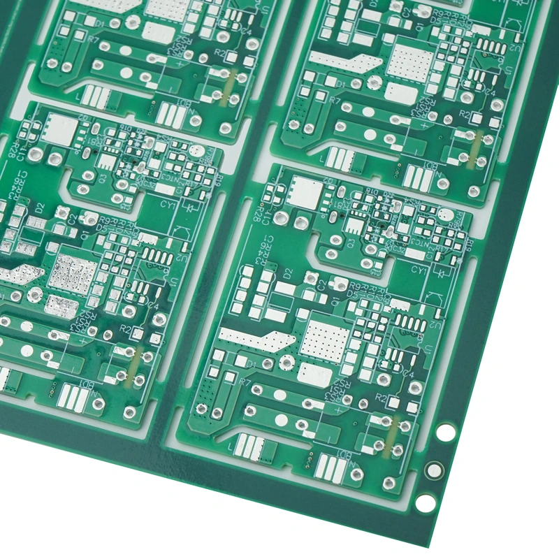
广德博亚新星电子科技有限公司 / Boystar PCB publishes bare-board examples for power, vehicle interfaces, industrial controls and appliances. The most useful distinctions are in its individual product notes: local 6 oz copper, a 10–14-layer / 3–4 oz construction, asymmetric A/B copper, resin-filled capped vias, plated edges and different surface finishes.
The company describes a business originating in Xianju, Zhejiang on 8 August 2008 and relocating to Guangde in 2015. The Guangde legal entity’s displayed licence instead gives incorporation on 6 November 2013. These describe different events; use the Guangde entity and producing address on the quotation.
COPPER / LOCAL, MULTILAYER AND ASYMMETRIC
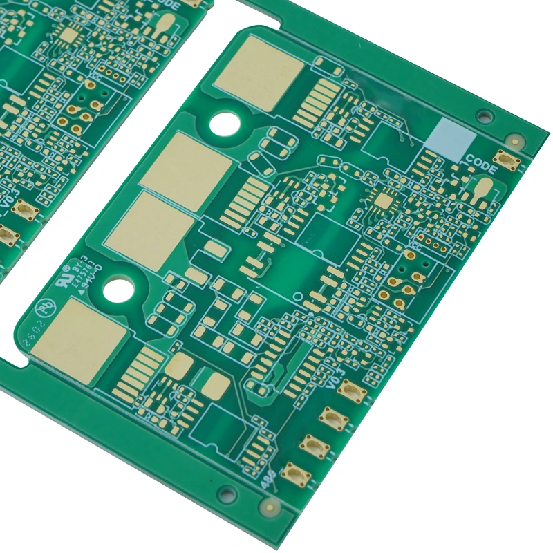
Three copper layouts. Three different DFM conversations.
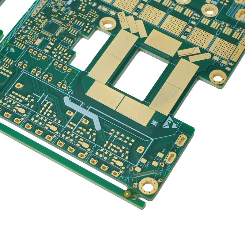
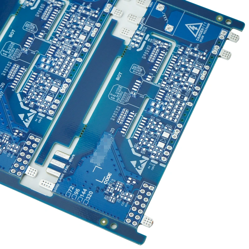
Local 6 oz copper PCB
Copper region
6 oz at the locally thickened positions
Laminate statement
High-Tg; no grade or numerical Tg supplied
Provide a copper-region drawing and transitions, not just “6 oz PCB”. Define whether the stated weight refers to starting or finished copper, acceptable height differences, local current/thermal paths and the exact high-Tg grade.
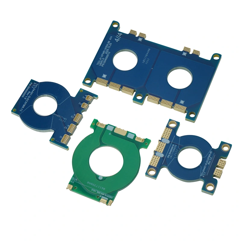
10–14-layer, 3–4 oz copper PCB
Published construction
10–14 layers
Copper statement
3–4 oz; layer allocation not specified
Release a layer-by-layer copper stack, insulation thickness, voltage conditions and winding/coupling requirements. Obtain DFM on etch compensation, press cycle and plated-hole geometry for that exact stack.
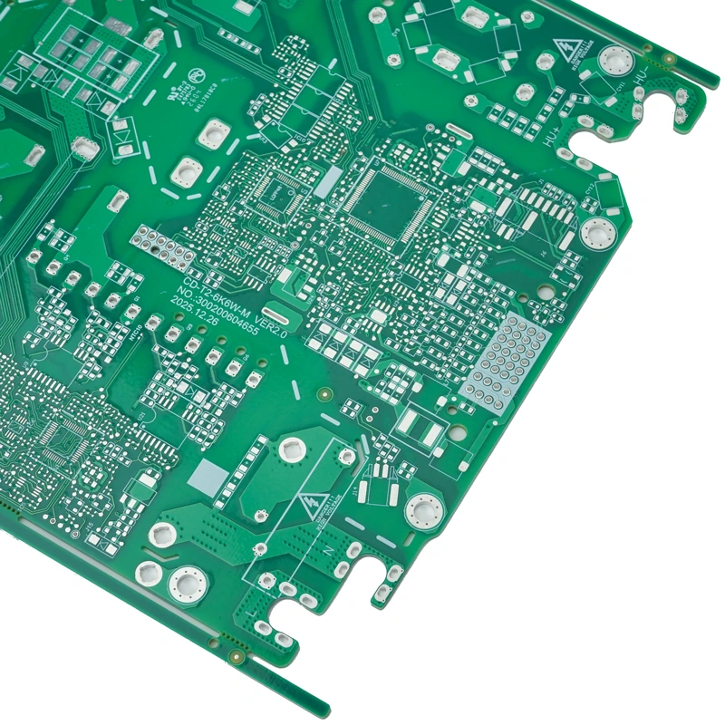
Asymmetric 1 oz / 2 oz power PCB
Copper statement
A side: 1 oz; B side: 2 oz
Signal requirement
Impedance design mentioned; no target or tolerance
Specify A/B orientation, starting versus finished copper, stack symmetry, bow/twist acceptance and reference planes. Ask for the proposed impedance stack and coupon; the application title does not supply a voltage or current rating.
What the published tolerances actually mean
The individual catalogue pages state line/space control tolerance ±10%, hole tolerance ±2 mil and board-thickness tolerance ±10%. These are not minimum trace/space dimensions, an impedance tolerance or a nominal board thickness. Agree the actual drawing values, measurement locations and acceptance method.
The 6 oz statement belongs to local positions; the 3–4 oz statement belongs to the 10–14-layer example; the 1 oz / 2 oz statement identifies A and B sides. Do not combine them into one fabrication envelope. The website does not define starting versus finished copper for these examples.
Supply the via map, filling material, cap thickness, planarity and solder-pad requirements. Specify the insulation and safety acceptance required by the charger design; do not infer an IPC via type or operating voltage from the photograph.
Four-layer halogen-free PCB with QR marking
Layers
4
Marking and material statement
Halogen-free; printed QR code
Name the laminate grade and the required halogen-free declaration. Release the QR content, serialization rules, print location and read-back acceptance. Define what the code links to: a printed code alone is not a complete lot-traceability system.
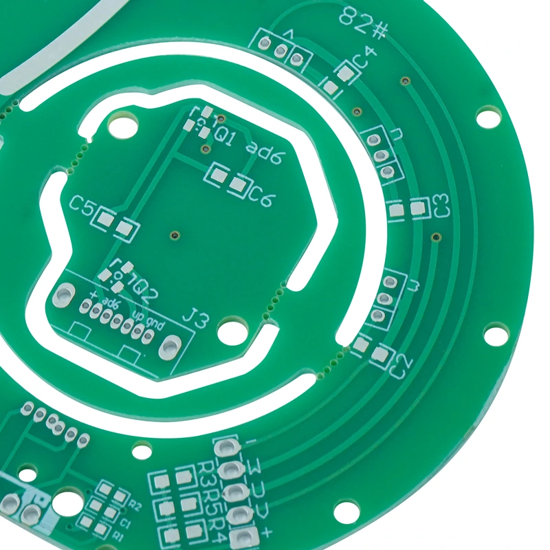
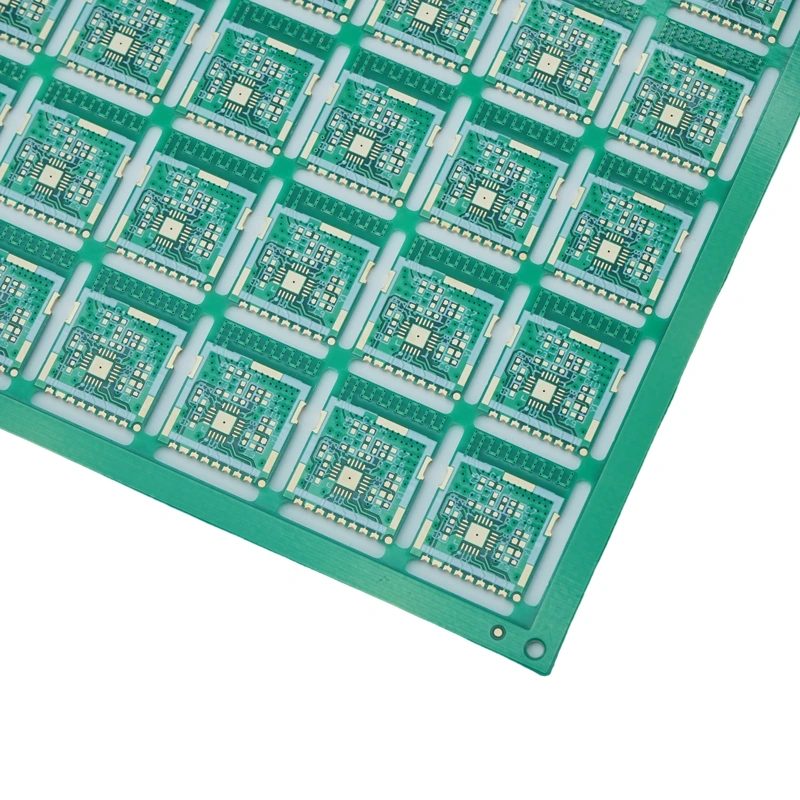
Double-sided HASL board with shaped outline
Construction
Double-sided; non-rectangular outline
Finish
Hot-air solder levelling; alloy not supplied
Specify the solder alloy and any lead-free requirement, surface flatness at fine-pitch pads, routed outline and plated/non-plated holes. Agree panel retention and dimensional inspection for the shaped board.
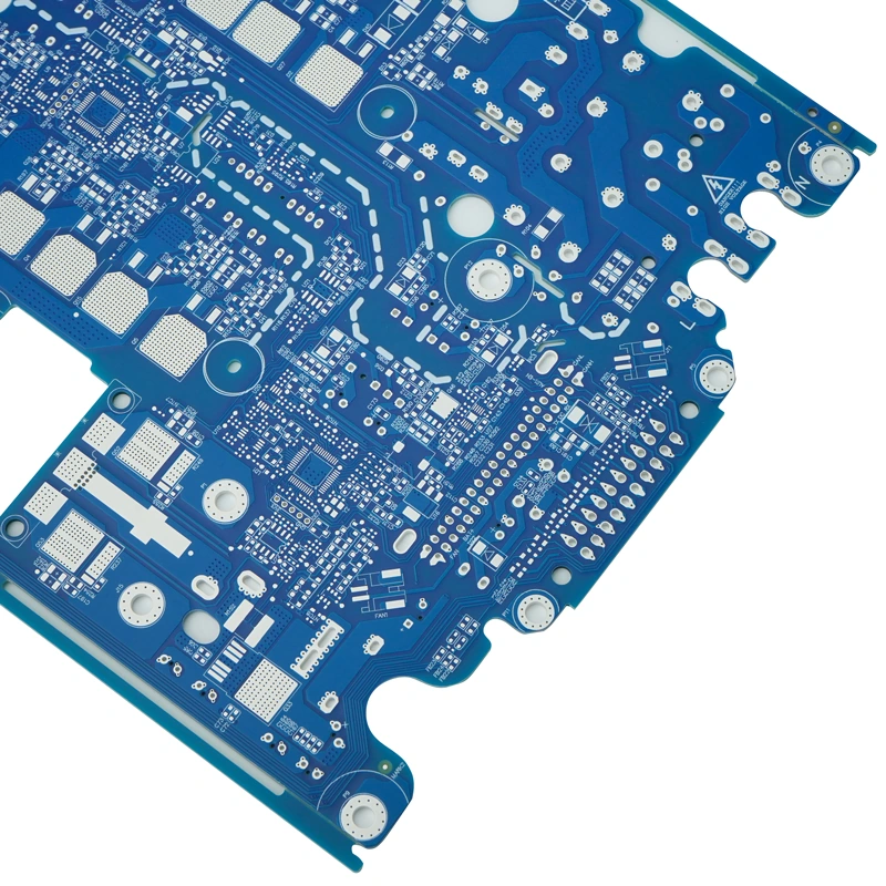
Matte-blue immersion-tin PCB
Finish
Immersion tin
Mask
Matte-blue solder mask
Release the tin thickness and inspection method, storage/shelf-life conditions and solderability acceptance after transport. State the mask specification separately; colour does not define the finish or laminate.
Keep material declarations and electrical targets separate.
“High-Tg” and “halogen-free” are source descriptions, not an identified laminate grade. Request the grade, thickness, supplier and required declaration for the actual order. Similarly, “impedance design” on power or communications examples does not give a target, tolerance, test coupon or reference plane.
For resin-filled, plated-over vias, release the hole structure and inspection requirements. For HASL or immersion tin, define alloy or finish thickness, planarity and solderability. A charging application does not establish the finished system’s operating voltage or safety approval.
INTERFACES / HOLES, EDGES, CONTACTS AND MASK
Release the mating feature before asking for a price.
Automotive USB-interface PCB
Published minimum hole
0.15 mm; drill versus finished-hole definition not stated
Application
Automotive USB interface
Clarify the 0.15 mm hole definition and its applicable board thickness and plating. Provide interface routing, connector dimensions, impedance targets and ESD/environmental requirements. No hole dimension is entered as a finished-hole limit until its definition is confirmed.
Metal-edged control-board example
Published edge feature
Metal edging and insertion pins
Dimensional detail
Edge coverage, contact metallurgy and tolerances not stated
Mark which edges must be plated and which must remain isolated. Include slot/edge drawings, bevels, creepage clearances, finish and connector mating tolerances. Obtain the panel route and inspection proposal before assuming all cut edges are plated.
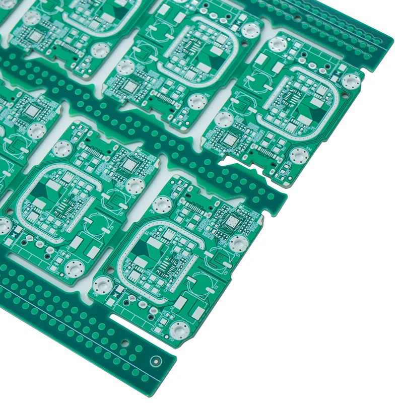
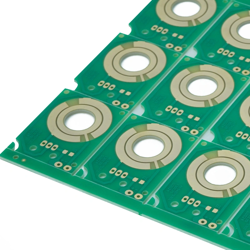
Half-hole lighting-control PCB
Edge interconnect
Half-hole process
Application
Lighting control
Supply the castellated-hole geometry, pad wrap, plated wall and burr requirements together with the mating assembly drawing. Specify whether electrical testing is performed before or after separation from the panel.
Automotive switch contact PCB
Gold statement
Gold thickness ≥0.05 µm
Wear statement
Wear resistance claimed; no cycle test conditions
Define nickel underplate, gold process, contact force, mating material and the required cycle/environment test. The thickness statement does not identify hard gold or prove a service-life cycle count.
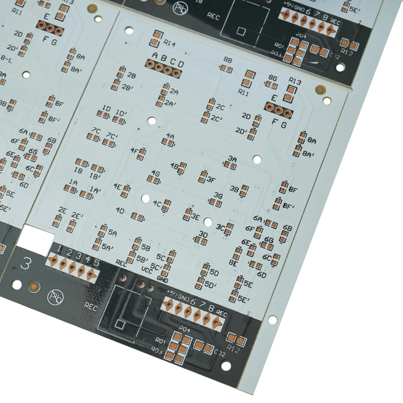
Two-colour solder-mask appliance PCB with OSP
Mask
Black/white split solder mask
Finish
OSP
Release the mask boundary/registration drawing, OSP specification, permitted thermal exposure and assembly/storage conditions. Define which surfaces require finish and which must remain masked; this is a fabrication example, not a populated appliance.
Finish, mask and contact life are different specifications.
The switch-board page states gold thickness ≥0.05 µm and claims wear resistance. It does not name hard gold, the nickel underplate, contact loading or a validated cycle count. Put those requirements into the contact design and acceptance plan.
The two-colour appliance example instead concerns mask registration and OSP. Keep the mask boundary, solderable area, storage and assembly exposure in the drawing. Neither an attractive board photograph nor an automotive application name establishes qualification for your programme.
The USB example’s 0.15 mm minimum hole has no explicit drilled/finished definition. It remains a source note rather than a finished-hole filter value.
PROCESS / IMAGING THROUGH ELECTRICAL ACCEPTANCE
Ask for the route and test coverage of your actual stack.
Image, drill and plate
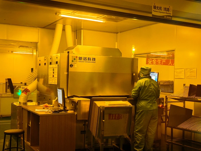
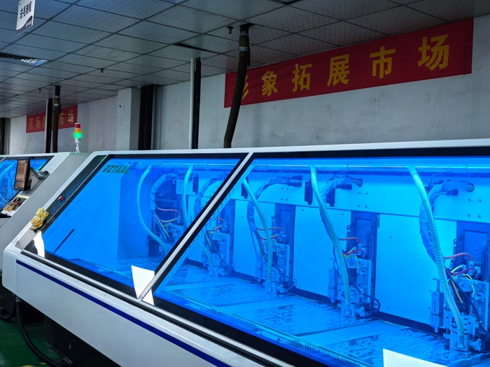
The original equipment galleries separately label exposure, drilling, copper deposition, electroplating, etching, character printing and OSP. The labelled automatic laser photoplotter produces imaging artwork; it is not evidence of a laser-drilling or HDI microvia process.
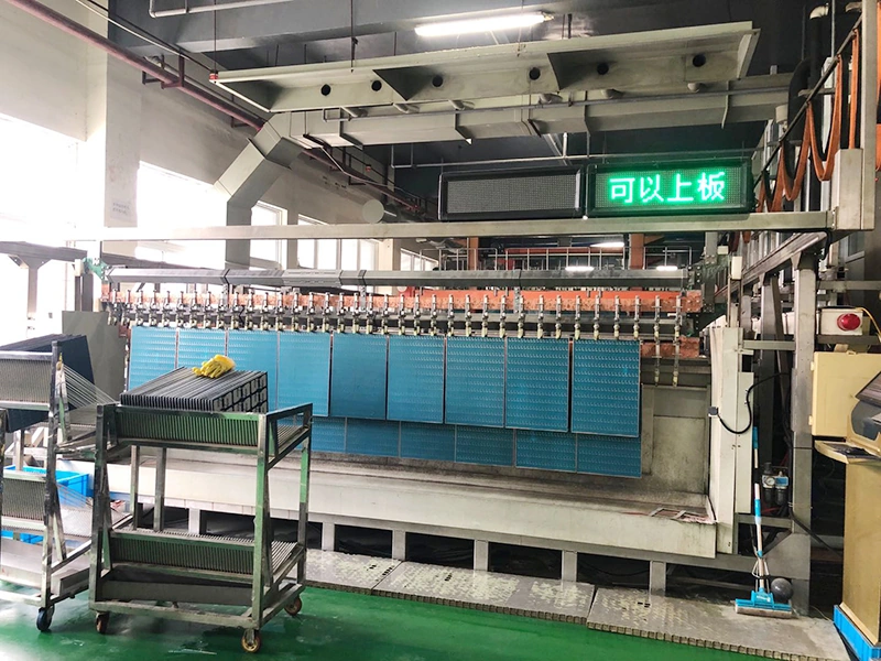
For thick or asymmetric copper, discuss image compensation, registration, copper build-up and press/drill controls. The newer gallery includes isolated equipment product illustrations; those do not independently demonstrate installation or utilisation. The photographs here come from the corresponding workshop-labelled entries.
Official exposure-equipment workshop entry; no registration accuracy inferred.
Official drilling-workshop entry; no laser-drilling capability inferred.Official automatic-electroplating-line entry; order-specific copper build-up still requires a process plan.
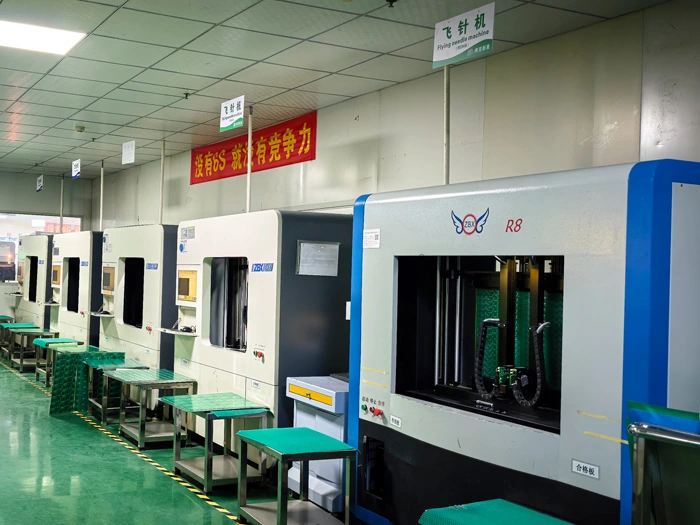
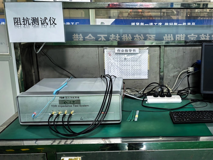
Manufacturer-labelled flying-probe equipment in the workshop gallery.Manufacturer-labelled impedance tester; no numerical impedance tolerance derived from the instrument photograph.
Turn equipment names into deliverables.
Specify the released netlist, open/short acceptance, test coverage and report format. For impedance work, define coupon design, measurement method, reference stack and lot reporting. For plated edges, capped vias and heavy copper, agree cross-section locations and dimensional/finish inspection. A machine name does not establish that every board receives the same inspection.
SUPPLYING ENTITY / GUANGDE AND DOCUMENT SCOPE
Match the contract, producing address and document scope.
Guangde supplying site
The official contact and licence identify the Guangde Economic Development Zone, Planning Road No. 1. The city’s 11 August 2023 police inspection publication matches the legal name, credit code 91341822082222087P and address. Its 23 June 2023 “no issues found” result concerns that police inspection; it is not a PCB process or product-quality approval.
The 2024 first-quarter environmental permit table also identifies the entity as electronic-circuit manufacturing. The displayed permit period ends on 22 July 2025, so that historical table is not presented as a current permit.
A 6 July 2026 occupational-health notice lists the same entity/address and records that required occupational-health examinations were not conducted. Its result column reads “无”; the record does not establish current remediation, a PCB-quality verdict or a blanket safety clearance. For programme due diligence, request the relevant current records and corrective-action status.
Manufacturer-hosted document copies
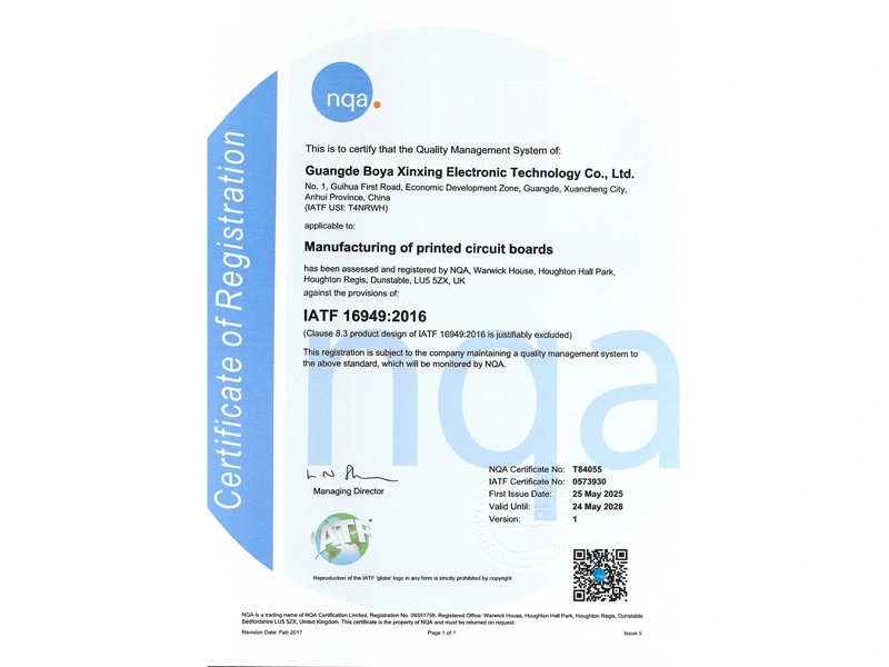
The displayed NQA IATF copy names the Guangde entity and printed-circuit-board manufacturing, certificate T84055 / IATF 0573930, valid 25 May 2025–24 May 2028. Product design is excluded. This describes the copy’s stated scope and dates; it is not a live issuer-status verification or approval of an individual board.
Manufacturer-hosted IATF document copy: printed-circuit-board manufacturing, with product design excluded.
UL, product and management-system document boundaries
The website’s UL screenshot names E475783 and the Guangde entity at No. 1 Guihua First Economic Development Zone. It is a manufacturer-hosted Product iQ copy last updated 15 May 2023, with separate single-layer and multilayer constructions. Do not apply its flame/thermal rows to every catalogue specimen or treat it as a current independent registry check.
The product-certification gallery has separate CQC documents for PCB constructions; these are not blanket approval of an assembled charger, vehicle controller or all laminates. The environment and occupational-health copies have their own management-system scopes. Request a readable current issuer record matching the producing site and construction required by your programme.
The high-tech-enterprise copy is dated 28 October 2025 and states a three-year period. This is a company recognition document, not proof of board geometry, automotive customer qualification or production yield.
ORDER RELEASE / CONSTRUCTION, INTERFACE AND ACCEPTANCE
A useful Boystar enquiry starts with one selected construction.
Fabrication revision: files, outline, quantities, panel and supplying entity/site.
Copper map: weights by layer and local region, starting/finished definition, laminate grade, insulation and stack symmetry.
Process outcome: resin fill/cap, finish chemistry and thickness, QR data/readability, halogen-free documentation.
Acceptance package: electrical netlist and test coverage, coupons/cross-sections, dimensional tolerances, lot records and programme-specific documents.
Reviewed 9 October 2026 against individual official product and equipment pages, their corresponding original photographs, displayed document copies and original Guangde government records. Product notes remain tied to their own examples; catalogue geometry is not inferred from photographs.
SOURCE TRAIL
Sources behind this profile
Individual review dated 9 October 2026. Local copper, plating zones and stack descriptions stay with their individual catalogue examples. Equipment photographs are distinguished from studio illustrations; government inspection records are not universal product-quality certification.