Automotive interfaces, wearable build-ups and microwave work call for different release packages.
Taizhou Botai Electronics Co., Ltd. (泰州市博泰电子有限公司) presents PCB design and manufacture at No. 10 Machuan Road, Yonganzhou, Gaogang District, Taizhou, Jiangsu. Its company introduction covers single-sided, double-sided and multilayer circuits and emphasizes microwave/high-frequency work. The individual product catalogue supplies a more concrete starting point: automotive display and junction-box boards, a twelve-layer multimedia construction, and four-, eight- and ten-layer wearable entries.
The useful comparison is not simply “up to twelve layers”. The display example needs a white-ink and assembly-interface review; the junction-box entry calls out countersunk holes; the thin ten-layer HDI entry specifies stacked vias and a named prepreg notation. Those requirements belong to their own constructions. This page keeps each photographed catalogue specimen with its published parameters and connects it to the information a purchasing team should release.
The company overview dates the Botai business to September 2005. Its history starts with a predecessor in September 2002 and a change of name in 2005; the overview and timeline also give different relocation years, 2009 and 2008 respectively. For a sourcing contract, use the supplying legal entity and current address rather than resolving that chronology into an invented incorporation date.
AUTOMOTIVE CATALOGUE / THREE DIFFERENT CONSTRUCTIONS
Separate the display finish from the junction-box holes and the multimedia stack.
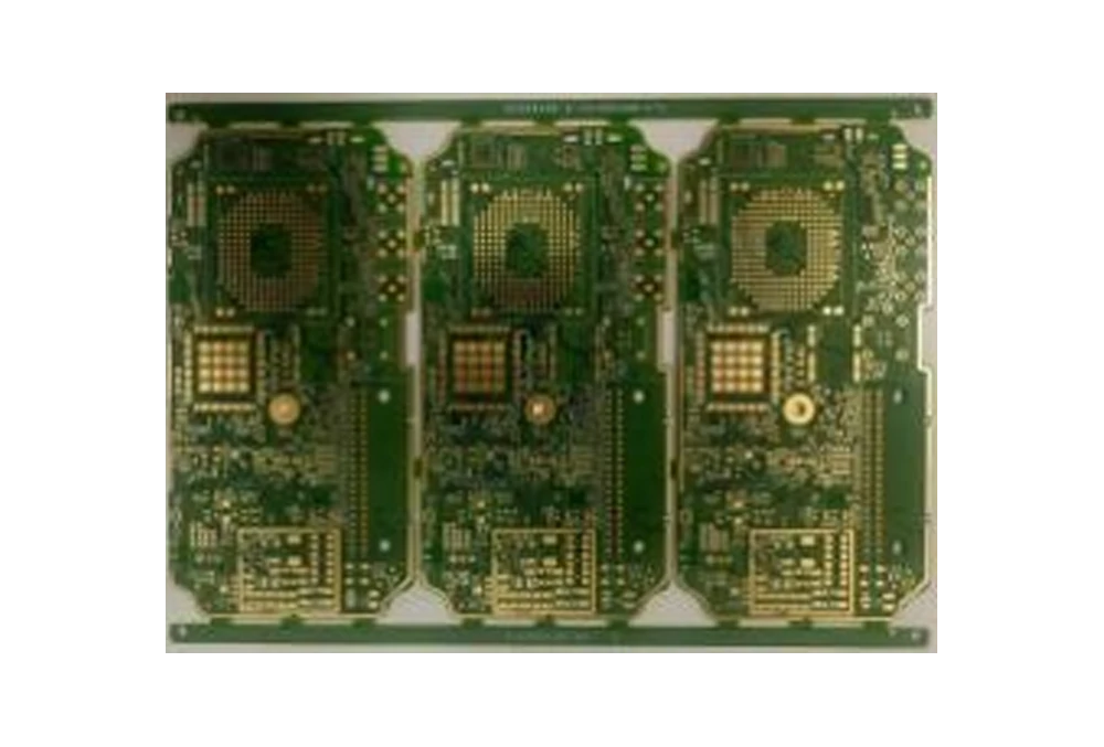
Automotive display · product 126. Complete manufacturer image; the source image itself is low resolution.
Four-layer automotive display board
Layers / thickness
4L / 0.6 mm
Trace / space
60 / 60 µm
Surface treatment
Immersion gold
Special process
White ink
The official page identifies a display application and a white-ink process. For a display assembly, state the required ink coverage, colour acceptance, pad openings and inspection method. Clarify whether any optical requirement applies to the bare board or to the finished assembly; the catalogue does not specify reflectance, colour tolerance or a populated display service.
Release the 0.6 mm stack, copper by layer, finished outline and handling requirements. Ask how panel support and dimensional inspection will be arranged for the actual assembly. The published conductor pair does not supply a finished-hole diameter or impedance tolerance.
Manufacturer-named “Automotive junction box” · product 134. Application follows the page text, not an inference from component footprints.
Six- to ten-layer junction-box entry
Layers / thickness
6–10L / 0.5–1.6 mm
Trace / space
100 / 100 µm
Surface treatment
Immersion gold
Special processes
Countersunk holes; resin plugging
A countersunk feature needs a dimensioned drawing: side, angle, depth, datum and the accepted remaining material. Identify which holes are plugged and specify their final condition. A “junction box” label cannot answer the mechanical and electrical interfaces to terminals, the enclosure or an assembled harness.
The layer and thickness ranges describe this catalogue family. Choose an actual stack and thickness for the quotation; do not assume every pair in those ranges is a released construction. State current, environmental and connection requirements so the supplier can propose copper and materials for that design. Neither current rating nor copper weight is published on this page.
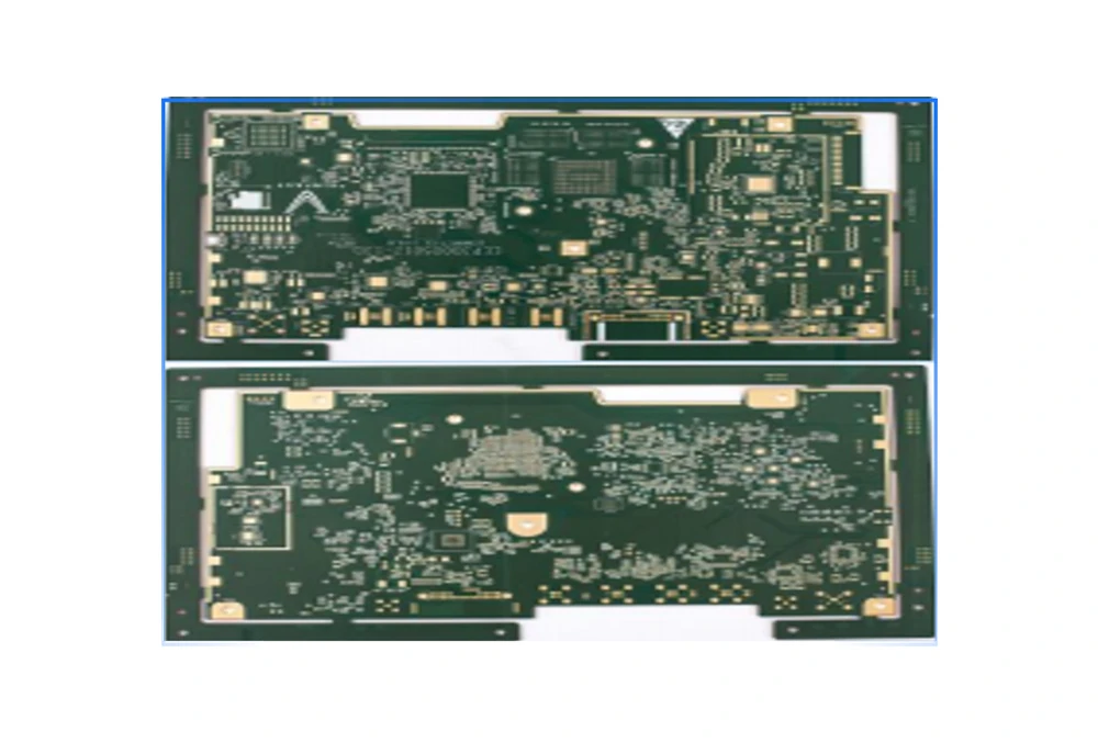
In-vehicle multimedia · product 127.
Twelve-layer multimedia construction
Build-up / thickness
12L (3+6+3) / 1.6 mm
Trace / space
60 / 60 µm
Surface treatment
Immersion gold
Special processes
Resin plugging; POFV
For this central-multimedia example, the manufacturer explicitly gives a 3+6+3 construction. Send a via table tied to that stack and mark the locations requiring resin plugging or POFV. Agree fill, planarization, pad condition and inspection evidence before accepting the process proposal.
The twelve-layer statement does not provide an impedance target, dielectric family, finished-hole limit or RF loss. For high-speed channels, release the target and tolerance with the proposed materials and ask for the coupon/report arrangement. Confirm connector geometry and assembly panel requirements separately.
WEARABLE CATALOGUE / BUILD-UP AND THICKNESS
A thin ten-layer stack is a different purchasing problem from a four-layer wearable.
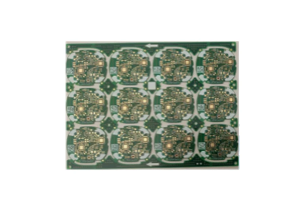
Sports wristband · product 131.
4L wristband: 1+2+1
Thickness
0.8 mm
Trace / space
60 / 60 µm
Finish
Immersion gold
Impedance tolerance
±8%, as published
The wristband entry is the one catalogue page here that publishes an impedance tolerance. Agree the actual impedance targets, stack, coupon and measurement method; ±8% alone is not a complete controlled-impedance requirement.
Define outline and connector tolerances and the assembly panel. The manufacturer calls the application a sports wristband and groups it under communication equipment; it does not provide a finished wearable's waterproofing or mechanical rating.
Page titled “Smart watch board” · product 133; its application text says “smartphone”.
8L entry: 2+4+2
Thickness
0.66 mm
Trace / space
60 / 60 µm
Finish
Immersion gold + OSP
Special process
Stacked-via design
The source's title and application disagree, so this is kept as an eight-layer catalogue construction rather than a claimed phone or watch customer reference. The stack, thickness, conductor pair, mixed finish and stacked-via wording are explicit.
Send the via connections and finish map. Identify which pads receive each treatment and agree solderability, storage and inspection requirements with the assembler. This page does not carry the four-layer wristband's ±8% impedance tolerance.
Smart watch · product 128.
10L watch board: 3+4+3 at 0.52 mm
Trace / space
45 / 45 µm
Finish
Immersion gold + OSP
Special notation
1017PP; stacked-via design
Published thickness
0.52 mm
The thinner ten-layer construction also has the finest explicit conductor pair in these six examples. The source prints “1017PP”, but does not identify a laminate manufacturer or complete material grade. Ask for the actual prepreg, resin content, pressed dielectric thickness and approved substitutions.
For a compact assembly, review the released build-up, copper balance, allowable bow/twist, pad coplanarity and panel support together. Request a via-fill and microsection acceptance plan appropriate to the specified connections. The photograph is not used to infer the smallest via or a reliability qualification.
MICROWAVE DIRECTION / SEPARATE PUBLIC RECORD
Ask for an RF construction and test method, not a transfer of the HDI limits.
Botai's company introduction emphasizes microwave high-frequency boards. Its timeline names a 2022 technical-renovation project for 5G microwave high-frequency composite ceramic substrates. This is the company's description of a project direction; its stated annual project scale is not treated as today's order capacity.
A 26 January 2025 report by the Taizhou Medical High-tech Zone / Gaogang Industry and Technology Innovation Bureau specifically names Botai's LV7700 microwave high-frequency electric-pulse composite circuit board as included in Jiangsu's 2024 new-technology/new-product promotion directory. That is a distinct named product record. It supplies no public laminate stack, conductor limit or loss measurement, and is not a factory quality certification.
An RF brief should identify operating bands, dielectric properties and allowable substitutions, copper and surface requirements, reference planes, connector transitions and the measurement arrangement. Ask whether a hybrid stack is proposed and how the quotation controls material lots and interface tolerances. Do not assign the wearable board's 45 µm conductor pair or the wristband's impedance tolerance to LV7700.
The catalogue also contains an entry titled “newly developed special military-industry product”, but its detail text publishes no specifications. An application label or general compliance statement does not establish permission to supply a regulated program. For that class of procurement, obtain the program-specific authorization and released requirements through the appropriate purchasing process.
Tie the quotation and inspection records to the Machuan Road factory.
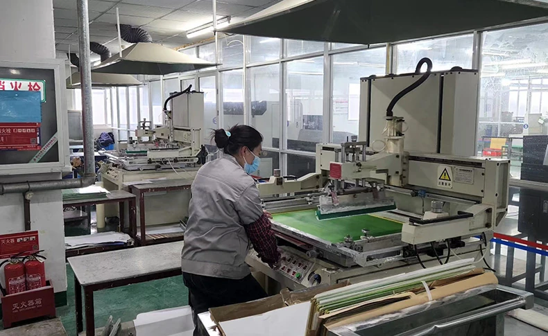
Official company page · “Processing workshop”. Equipment models, counts and current line availability are not inferred from the photograph.
The overview describes approximately 38 mu of land and 25,000 m² of buildings, a claimed daily capacity above 1,200 m² and monthly capacity of 30,000 m². These are manufacturer-published scale statements, not measured utilization or a committed delivery window. Request a schedule for the selected construction, quantity and qualification stage.
The website presents workshop and development photographs but no detailed, dated equipment inventory alongside these product entries. For a stacked-via order, ask which drilling, filling, planarization and inspection operations support the proposed stack, where they take place and which records are delivered. A workshop photo does not supply a machine specification.
The official contact page gives botaipcb@botaipcb.cn, 0523-82378388 / 86988089 and the Machuan Road address. These are published contact details; no email or mailbox-control test was performed. Ask for the entity name on the quotation, invoicing and shipment paperwork before an order is released.
Before approving the build
Agree the selected catalogue construction and your order-specific stack, quantities and delivery stages.
Release via, hole and finish maps; state thickness, dimensional and assembly acceptance criteria.
Specify electrical testing, microsections and any impedance or RF measurement deliverables.
Record material substitutions, lot traceability and the response to an engineering change.
POSTED DOCUMENTS / DATE AND MANUFACTURING SCOPE
Read the current copy, the date and the site before using a qualification.
IATF 16949 copy
The manufacturer-hosted Chinese Bureau Veritas copy identifies Botai at No. 10 Machuan Road, USI 6ZR2RC, IATF certificate 0548746 and reference CN052321–IATF. It prints validity 5 October 2024–4 October 2027, PCB manufacturing scope and exclusion of product/service design and development.
The copy says the formal certificate is English and that this Chinese text is a reference. Obtain the current formal certificate and issuer status for the supplying site. The document does not approve a vehicle program or each photographed board.
Three ISO copies: renewal needed for a current review
The ZRX-issued copies posted by Botai cover ISO 9001 (07623Q1628R1M), ISO 14001 (07623E0914R1M) and ISO 45001 (07623S0801R1M). They identify the same entity, code 91321203782711922T, and Machuan Road operating site.
Their scopes concern high-frequency-board design, production and after-sales service, with environmental or occupational-health activities as appropriate. Each visible copy prints 2 July 2026 as its expiry, preceding this page's research date. Request renewed documents; these copies are not displayed as currently valid qualifications.
The overview mentions US UL standards and hazardous-substance process controls, but the reviewed certificate catalogue does not supply a UL file with an ownership match or a product-specific material declaration. Ask for the applicable file/site/construction and material records for the order. Manufacturer-hosted documents are described as copies; no independent-certification badge is inferred.
Individually researched 8 October 2026. Each named product detail and its original photograph was reviewed, along with the company, contact, workshop photograph and four full certificate copies. The government report was read independently. Numeric fields stay with the named construction; unknown finished-hole and material-grade fields are not inferred from photographs. Purchasing questions are editorial guidance, not additional factory specifications.