

What this manufacturer makes
Aoshikang manufactures circuit boards for automotive electronics, servers and storage, telecommunications and digital energy. Its technical offering includes backdrilling, controlled impedance, mixed-material construction and embedded features. Published support specifications cover high-layer fabrication, interlayer alignment and signal-loss test methods.
Official company source reviewed- Manufacturing focus
- Server & storage PCB · Automotive electronics · RF & digital energy
- Published footprint
- Hunan · Guangdong; confirm the production base
Multilayer PCB — technical-support envelope
Manufacturer reportedAoshikang’s technical-support table specifies a 24-layer ceiling, aspect ratio up to 21:1 and ±8% impedance tolerance. It lists backdrill stubs of 2–10 mil and signal-loss methods including SET2DIL, Delta-L and TRL. The separate “24+” heading does not establish a higher numerical production limit.
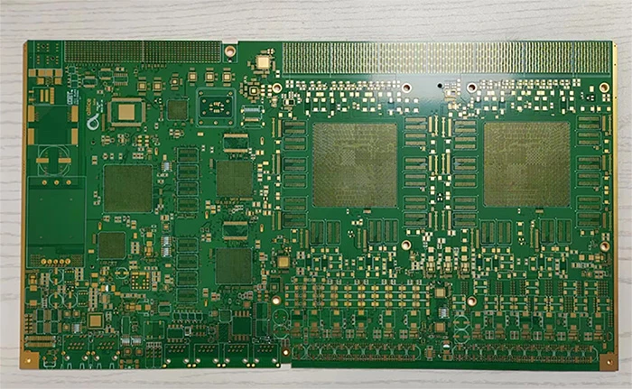
Technical-support table says 24L while another heading says 24+. Only the explicit table limit is used; no lower layer bound is assumed.
- Layer count
- Up to 24 layers
- Line / space
- —
- Finished hole
- —
- Impedance
- ±8%
| Maximum layers in table | 24 |
|---|---|
| Impedance tolerance | ±8% |
| Aspect ratio | ≤21:1 |
| Backdrill stub | 2–10 mil |
| Loss testing | SET2DIL, Delta-L and TRL listed |
| Technical source | askpcb.com · Manufacturer specification |
Published limits may refer to different constructions. Confirm the complete stack-up with the factory. A dash means no value was published.
Sources & review record.
Reviewed 2026-09-21. Manufacturer pages can change; confirm the current revision when requesting a quotation.
- 市场https://www.askpcb.com/enmarket/Source checked 2026-09-21Official website
- 技术支持https://www.askpcb.com/enservice/support.htmlSource checked 2026-09-21Official website
Make the first technical conversation useful.
Which insertion-loss method, stub target and coupon design apply to the proposed stack-up and operating frequency?
Attach the manufacturing brief
Layer stack-up, finished dimensions, copper weights, laminate grade, quantity and delivery destination.
Define acceptance
Finished-hole tolerance, impedance targets, coupon requirements, surface finish and permitted process substitutions.
Confirm the recipient
Agree the manufacturing legal entity, confidentiality terms and approved site before sharing production files.