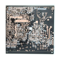
1POY030273A · single-sided power board
- 1 layer
- OSP
- Published hole: 0.80 mm; finished/drilled basis unspecified
Specify insulation, copper, creepage and clearance, mounting and circuit-side acceptance.


MANUFACTURER DOSSIER
深圳市中络电子有限公司 · Guangdong
Shenzhen Zhongluo Electronics Co., Ltd. · 深圳市中络电子有限公司 dates its establishment to 10 March 1997. The official contact address is No. 5 Niusheng Road, Xiuxin Industrial Area, Kengzi, Pingshan, Shenzhen. Its introduction distinguishes single-sided fabrication, double-sided/multilayer fabrication, lamination and CNC drilling departments.
The catalogue is unusually useful for separating sourcing questions: single-sided power boards, two-sided charging and half-hole panels, four-to-eight-layer impedance examples, and aluminium or copper-base constructions. The general process table extends to 16 layers, but that ceiling is separate from the photographed catalogue examples.
Choose the route that fits your fabrication drawing. A power-board model, a BGA example and a copper-base thermal board need different material, interconnection and acceptance instructions. None is a substitute specification for the other.
The single-sided catalogue identifies power-supply applications; the two-sided catalogue adds small charging boards and a half-hole panel. Customer/application labels in the source describe those examples, not a current endorsement or approved-vendor relationship.
Specify insulation, copper, creepage and clearance, mounting and circuit-side acceptance.
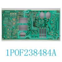
Release the power-supply layout, laminate grade and flame/safety requirements for your product.
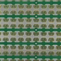
Define delivery panel, break-off method, electrical test and finished plated-hole drawing.
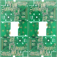
Confirm the model revision, circuit-side data, spacing, stack thickness and gold-finish acceptance.
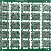
Define castellated-edge geometry, plating, burr limits and the assembly-facing delivery panel.
The two-sided page labels two different photographs 2PGG620028A with the same specifications. This profile keeps one model entry. The other image's filename is not used to invent a second model number.
For half-hole edges, add the edge plating, opening position, burr limits and delivery panel to the drawing. For charging-board arrays, agree rails, fiducials, break-off method and whether electrical test is reported per circuit or per panel.
The manufacturer's catalogue pairs layer counts with finish, line width and solder-mask bridge values. It does not give a numerical impedance tolerance or a laminate stack for these models. Solder-mask bridge is not copper trace spacing. The quoted product “hole” values are retained as source wording; they are not entered as confirmed finished-hole limits.
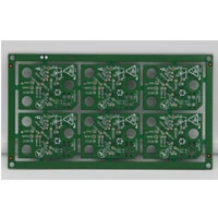
Send the four-layer stack, impedance net classes, targets, tolerance and coupon requirements.
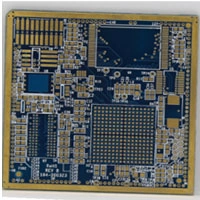
Agree BGA escape routing, via construction, mask registration and a stack-specific impedance test.
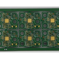
Release the six-layer signal/reference assignment and finished-hole requirements before quoting.
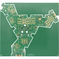
Confirm HDI build-up/via structure and selectively plated gold thickness and areas.
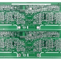
Specify thick-board drilling, aspect ratio, plating, bow and mechanical-fit tolerances.
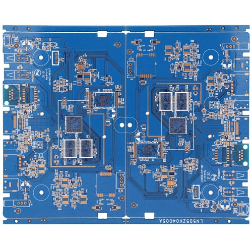
Agree the OSP handling/storage requirement alongside the impedance stack and acceptance coupon.
The eight-layer BGA entry reports a 0.10 mm line and 0.15 mm hole; the separate eight-layer HDI entry reports a 0.125 mm line and a thick-gold/immersion-gold finish combination. The 2.5 mm thickness belongs to a four-layer model. They are three different catalogue constructions, not one demonstrated eight-layer HDI specification.
For an impedance RFQ, send net classes, targets, tolerance, reference layers, stack-up and coupon requirements. For the HDI model, ask engineering for the actual build-up and via structure; the title alone does not disclose laser-via dimensions or sequential-lamination cycles. Define selective gold thickness and plated areas separately from immersion gold.
Read the construction text rather than the category heading. Two examples are explicitly described as copper-base; one is aluminium-base. The source does not publish a dielectric grade, thermal conductivity, dielectric withstand voltage or interface thermal resistance for these boards.
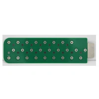
Define copper-base thickness, dielectric isolation, heat path and mechanical joining process.
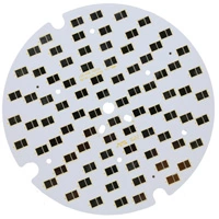
Require a named thermal dielectric and test conditions, rather than a high-conductivity label alone.
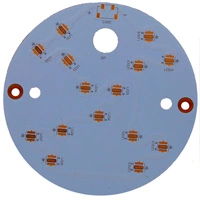
Provide countersink angle/depth, mounting contact, isolation and flatness acceptance.
For a thermal design, specify the metal base, dielectric supplier/grade and thickness, copper, isolation voltage, heat path and mounting interface. Request a construction-specific thermal and electrical response. “High thermal conductivity” in a model description is not a numerical W/m·K guarantee.
The table's ±20% line-width tolerance (special ±10%) is a dimensional value, not an impedance tolerance. Its 450 × 965 mm entry belongs to the electrical-test board-size section; it is not promoted as the maximum finished production board.
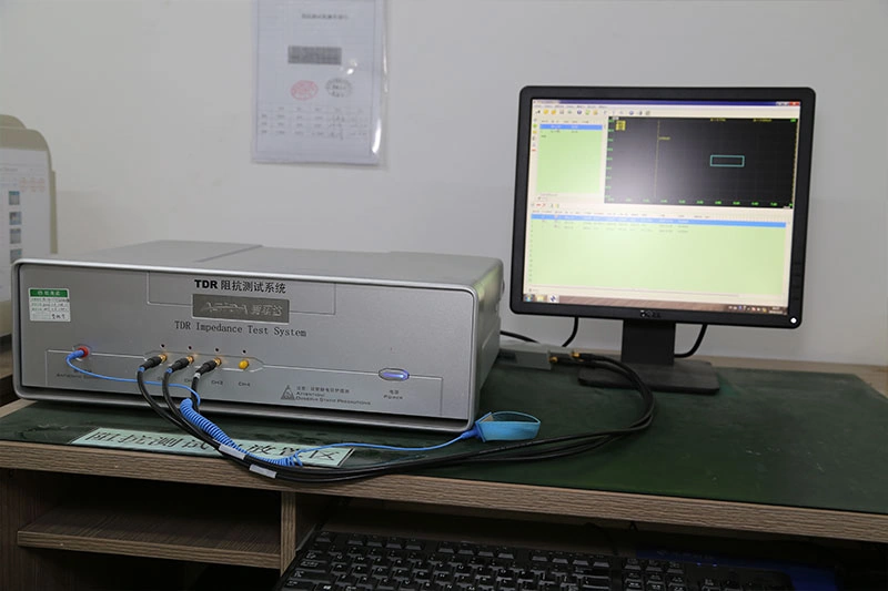
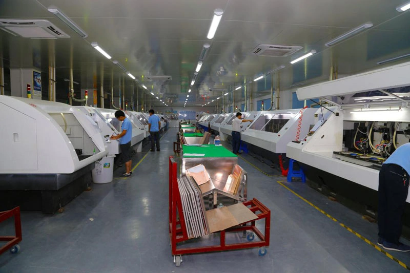
The gallery captions name single-sided automation, punch and alignment equipment, automated testing, brushing, automated copper/tin plating, AOI and CNC routing. Separate flowcharts describe single-sided, double-sided and multilayer fabrication. The diagrams branch by surface finish before profiling, electrical test, final inspection and packing.
Ask which steps take place at the supplying site and where outsourced operations enter the control plan. Photographs do not establish available machine hours or a reserved delivery slot.
The testing gallery names four-wire low-resistance testing, AOI, RoHS instrumentation, a UV spectrophotometer, automated visual inspection, TDR, an eight-zone reflow unit and a handheld copper-thickness tester. A reflow photograph does not establish a turnkey PCBA service for this board catalogue.
The electrical-test table prints “MAX 50 MΩ” for insulation, “MIN 20 Ω” for continuity and “MIN 10 µA” for leakage. Those directions are ambiguous as acceptance limits. Obtain a reviewed netlist test programme with agreed pass/fail thresholds instead of copying them into a purchase order.
The delivery page makes its windows conditional on material being ready and engineering queries (EQ) being confirmed. It distinguishes samples, first production and repeat orders. The page does not say these are calendar days or working days; agree the counting basis, start event and dispatch milestone.
Samples: 2–5 days
First production: 5–10 days
Repeat production: 3–7 days
Samples: 3–6 days
First production: 5–10 days
Repeat production: 5–9 days
Samples: 8–12 days
First production: 12–15 days
Repeat production: 10–12 days
The official contact page publishes marketing@zhongluodz.com. Publication of the address has been checked; mailbox control has not been tested. Keep the shortlist and initial fabrication brief on PCBVerified.
Prepare the Zhongluo RFQ →The displayed ISO 9001:2008 certificate names the company and expires on 23 July 2019. The ISO 14001:2004 copy expires on 21 May 2018. They are historical documents, not current certification badges.
Three UL report excerpts show E255554, with 2016 revisions/issue dates and construction types ZL-01 to ZL-08. They are individual parameter pages, not a current holder record or authorization for every board. The CQC copy shows CQC15001134930, issued 6 July 2016. Request current issuer status, construction scope and the matching supplying address.
Shenzhen's second 2025 environmental-credit list, using data through 31 March 2025, lists 深圳市中络电子有限公司, code 914403007152917612, Pingshan, as “环保警示企业” (environmental warning). The fourth 2025 list, using data through 30 September 2025, lists the same entity as “环保良好企业” (environmental good).
Both original records are retained. The later classification does not establish today's permit status or prove closure of a specific historical issue. For supplier qualification, obtain the current site permit and monitoring information.
The undated introduction reports 37,000 m² and 500 employees, with annual single/double/multilayer figures of 1.8 million / 400,000 / 200,000 m². The homepage instead reports 500,000 m² for double-sided boards. The delivery page gives monthly figures of 150,000 / 25,000 / 15,000 m². These different reporting bases have not been converted into one current capacity claim. Ask for the actual route, utilization and available order slot.
Individually researched 9 October 2026. Four product catalogues, their complete original images, process/test tables, six document images and both complete government lists were read. Fourteen distinct product constructions are preserved; one repeated model label is not counted twice. Product hole values remain descriptive because finished-hole status is undefined. The numeric impedance filter stays empty.
We use cookies to provide our services and measure website usage. Privacy policy