YUEJIE / FROM CATALOGUE TO CONTROLLED CONSTRUCTION
Choose the fabrication route before comparing the headline limits.
Yuejie’s Chinese website presents multilayer, HDI, RF, flexible and heavy-copper PCB families. The useful distinction is between a catalogue reference and a process envelope. Six original family images below help explain what to specify; they do not come with a complete, individual fabrication drawing.
The general rigid table separates standard capability from sample limits. The FPC page uses sample and volume columns in the opposite order. Keep these labels with the numbers when preparing a drawing review.
CONTRACTING PARTY / CHECK THE NAME AND ADDRESS
Dongguan company name, Shenzhen contact, Rocket PCB connection.
What the manufacturer publishes
The contact page names 东莞市跃捷电路科技有限公司 and gives B301, Building B, Huafeng Technology Park shops, Yanchuan, Yanluo, Bao’an, Shenzhen. It lists 4008-086-528, mobile 15013510516 and sales-sz@rocket-pcb.com. This is a published contact address, not proof that every listed process is performed there.
The rigid-flex capability page instead names 跃捷电路科技(深圳)有限公司. The bonding-board page contains a combined, inconsistent company string. Obtain the exact registered contracting entity, beneficiary and producing-site allocation; those names are not silently merged into a group.
Official screening record
OFAC’s 1 October 2025 designation names Rocket PCB Solution Ltd and the exact Dongguan Chinese company. The live detail record 55444, read on 9 October 2026, lists Rocket PCB on the SDN list under IFSR and NPWMD, USCC 91441900595831304L, and a corresponding Shenzhen address. It also contains secondary-sanctions information.
Check the current official record and transaction-specific requirements before contracting, payment or sharing controlled files. This research page establishes no permission to transact.
Read the rigid envelope beside the actual stack and copper.
Standard column
Maximum rigid layers
64
Rigid thickness
0.2–10.0 mm
Line / space
70 / 70 µm
Mechanical / laser hole
200 / 100 µm; finished-hole definition not supplied
Copper range
1/5–10 oz
Impedance tolerance row
±8%
HDI structure row
3 + N + 3
Sample-limit column
Maximum rigid layers
68
Rigid thickness
0.1–14.0 mm
Line / space
50 / 50 µm
Mechanical / laser hole
150 / 100 µm; finished-hole definition not supplied
Copper range
1/7–12 oz
Impedance tolerance row
±5%
HDI structure row
4 + N + 3, as printed
The source also varies usable length and width by multilayer construction. Request a panel drawing with margins and handling requirements. Its aspect-ratio entries are printed “01:16” and “01:18”; confirm their intended definition rather than silently reformatting them as an accepted board specification. Routing and impedance limits need the actual copper, dielectric, coupon and measurement conditions.
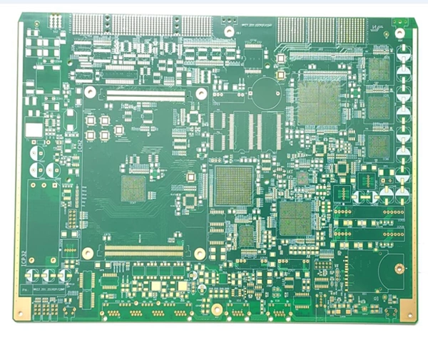
Original Yuejie technology-family photograph, without crop. Exact sample layers, laminate, copper and routing are not disclosed.
Multilayer PCB — catalogue reference
Published family
Multilayer PCB
Catalogue date
16 March 2022
Pictured construction
No individual stack or dimensions disclosed
Request a controlled stack, laminate grade, finished copper, finished holes and a manufacturing-site allocation. The family page’s 64-layer headline is not this photograph’s layer count.
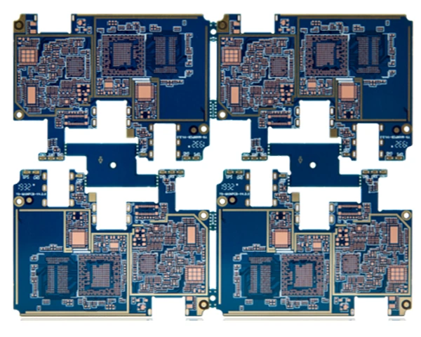
Original Yuejie technology-family photograph, without crop. Exact sample layers, laminate, copper and routing are not disclosed.
HDI PCB — catalogue reference
Published family
HDI / any-layer
Catalogue date
16 March 2022
Build-up and filled vias
Family description; sample construction unspecified
Release the build-up sequence, dielectric per cycle, laser-via and pad dimensions, fill/cap acceptance and coupon sections. Confirm the detailed rule instead of relying on the inconsistent 0.0275-inch text.
Resolve the HDI text before selecting a build-up.
The HDI family page describes up to 40 layers and sequential lamination. It also prints 0.0275-inch trace/space, while the general table uses 70 µm standard and 50 µm sample routing. These are not treated as equivalent numbers or corrected into a more attractive limit. The unavailable parameter-image URLs do not supply an independently readable HDI table. Ask for the approved build-up and dimensioned microvia section.
RF1-2 / RELEASE THE MATERIAL PAIR BY LAYER
A hybrid laminate needs more than a “Rogers” label.
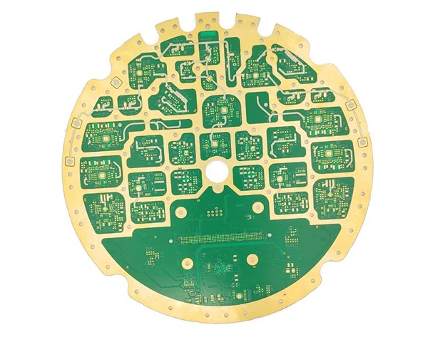
Original Yuejie technology-family photograph, without crop. Exact sample layers, laminate, copper and routing are not disclosed.
RF1-2 mixed-material PCB — catalogue reference
Source identification
RF1-2
Published family
Mixed high-frequency laminate
Material pair / layers
Not assigned to the pictured board
Specify the actual RF and FR-4 grades by layer, dielectric thickness, copper treatment and registration allowance. The example material pairs on the page do not establish this sample’s bill of materials.
Material and bonding instruction
The hybrid page discusses combinations such as RO4350B with IT180A, 370HR, NP175FR or TU768. These are example combinations in the family description, not this photograph’s disclosed material list or evidence of current stock. Specify the actual core and bonding material, thickness and copper treatment for each layer.
Registration and electrical acceptance
The source discusses differing material expansion and registration through lamination. Agree the stack, hole treatment, finished geometry, RF coupon and acceptance at the operating band. A general catalogue entry does not establish measured insertion loss or the delivered board’s dielectric properties.
The high-frequency family page has a long material table, including Rogers, Panasonic, Isola, Arlon and other supplier names. A listed grade is a sourcing enquiry, not a batch certificate or authorised-distributor proof. Request a traceable laminate record for the actual order.
FLEX / ZONE-SPECIFIC STACK AND BEND DUTY
Separate a flexible circuit from the rigid portion of a rigid-flex board.
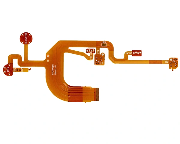
Original Yuejie technology-family photograph, without crop. Exact sample layers, laminate, copper and routing are not disclosed.
Flexible PCB — catalogue reference
Published family
Flexible circuit
Substrate discussion
PI / PET families
Pictured flex stack
Not specified
Release the copper type, adhesive construction, coverlay/stiffener zones, bend radius and static or dynamic duty. Generic claims about bending cycles are not this circuit’s test result.
FPC sample versus volume
Layer range
Sample 1–8; volume 1–6
Thickness
Sample 0.06–1.0 mm; volume 0.08–0.8 mm
Line / space
0.045 / 0.045 mm in both columns
Material families
PI / PET, RA / ED copper; individual stack not assigned
Published impedance range
50–120 Ω — a target range, not a tolerance
Hole row
CNC 0.15 mm / laser 0.10 mm; not defined as finished diameter
The table lists 12, 18, 36 and 70 µm copper and separate dielectric thicknesses. Release the actual copper and adhesive construction. Its long 250 × 4000 mm size entry requires confirmation of usable product length, panel processing and handling. Generic repeated-bending language is not a fatigue report for the pictured flex.
Original Yuejie technology-family photograph, without crop. Exact sample layers, laminate, copper and routing are not disclosed.
Rigid-flex PCB — catalogue reference
Published family
Rigid-flex PCB
Catalogue date
16 March 2022
Rigid and flexible zones
Separate construction needed
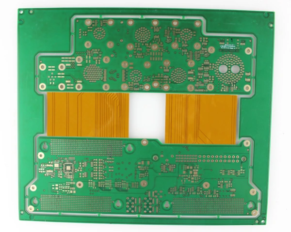
Define the rigid/flex stack by zone, cavity and transition geometry, bend use, coverlay and plated-hole placement. Clarify the producing legal entity: the linked rigid-flex process page carries a different Shenzhen company name.
The separate rigid-flex table states 2–24 layers in the rigid portion and 1–6 in the flexible portion, 0.075 / 0.075 mm line/space and 0.20 mm minimum mechanical drilling. These zones are not added together to invent a total layer count. Its overall-thickness row is printed “0.4 mm to 3 metres”; that unit error is not silently changed to 3 mm. Ask for the controlled zone thickness, coverlay, transition and bend requirements.
POWER / RESOLVE THE COPPER ENVELOPE CONFLICT
Heavy copper needs its own routing and lamination review.
Original Yuejie technology-family photograph, without crop. Exact sample layers, laminate, copper and routing are not disclosed.
Heavy-copper PCB — catalogue reference
Published family
Heavy copper
Copper statement
Family text: up to 10 oz inner / 20 oz outer
Pictured board copper
Not specified
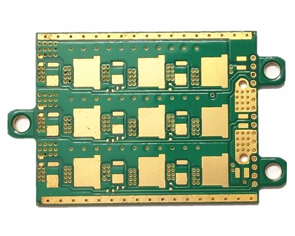
Give finished copper per layer, routing at that copper thickness, current/temperature conditions and a resin-fill and plated-hole acceptance plan. The 20 oz family claim exceeds the general 12 oz sample column and needs a construction-specific review.
The heavy-copper family text advertises 10 oz inner and 20 oz outer copper, whereas the general sample table tops out at 12 oz. Keep the discrepancy visible in the drawing review. Neither number is assigned to the pictured board, and neither establishes its current rating or temperature rise.
Copper definition: specify starting foil and finished copper on every layer, including local plating and connection zones.
Etching and resin fill: release line/space at that copper, copper distribution, prepreg and void acceptance.
Holes and terminals: define finished holes, plated-wall copper, terminal positions and thermal/mechanical loading.
Inspection: agree dimensional and cross-section reports against the actual heavy-copper construction.
PROCESS GALLERY / PHOTOGRAPHS AND DOCUMENTS HAVE DIFFERENT ROLES
Use the equipment gallery to ask where each operation happens.
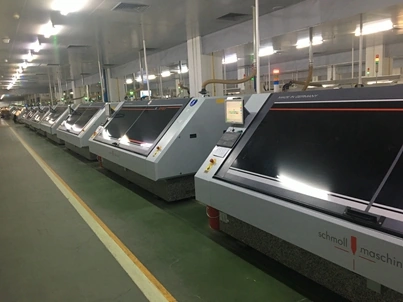
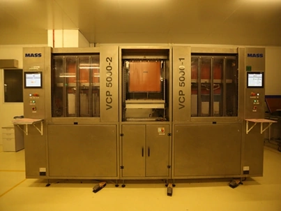
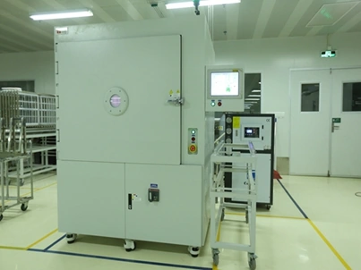
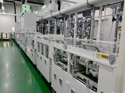
Official equipment gallery — labelled laser drilling; site, model and installed quantity are not specified.Official equipment gallery — labelled VCP; no production-capacity value is inferred.Official equipment gallery — labelled plasma processing.Official equipment gallery — labelled DES line.
The gallery also labels high-speed drilling, routing, exposure, automatic LDI and automatic testing. Some images are low resolution, and the reviewed page does not allocate them to a named producing site. Confirm the order’s process route and test coverage, with current evidence for the responsible facility. The photos are not an independent equipment audit.
A certification logo is not a scoped certificate.
The “quality certification” page shows a collage of ISO, IATF, AS9100, SGS and other marks. It provides no readable holder, site, certificate number, validity or product scope. No current certification badge or UL file is assigned from that image. Request the applicable issuer record for your producing entity and construction.
The delivery page provides a schedule image and the homepage advertises expedited service. Treat these as published planning material. Material procurement, engineering clearance, process cycles, inspection, quantity and the actual release date must be included in a current schedule; no delivery or quote-response guarantee is made here.
ENGINEERING RELEASE / A PRECISE NEXT STEP
Make the specification answer the route’s unresolved questions.
Rigid, HDI and hybrid RF
Send the revision-controlled Gerber, drill and netlist, stack by layer, starting/finished copper, laminate and bondply grades, build-up sequence, hole definitions and impedance/coupon plan. Resolve standard versus sample requirements and each contradictory notation.
Flexible and power constructions
Add zone drawings, bend duty, coverlay/stiffeners and transition geometry for flex; copper-specific routing, resin fill, terminal loading and inspection for power boards. Identify the exact producing entity, site and order-specific qualification requirements.
Reviewed 9 October 2026. Six catalogue references retain their individual source images and unknown sample geometry. The company-introduction and ceramic-product pages returned 404; unavailable parameter images are not reconstructed from filenames or marketing headlines.
SOURCE TRAIL
Sources behind this profile
Original manufacturer pages, corresponding uncut catalogue images and the original OFAC records were read separately. A family limit, equipment photograph or certification logo is not a construction-specific qualification. Dates and unresolved definitions remain attached to their sources.