

Match the application before using a process maximum.
These are the two manufacturer catalogue entries reviewed here. Their detail pages identify the application and show original board panels, but do not specify an individual stackup, copper weight, finished thickness or material grade. The process figures further down describe separate manufacturing routes.
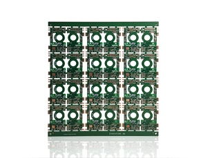
Power supply & new energy
Use this entry to start a power-board discussion. Send the current path and starting/finished copper for every layer, the dielectric stack, local copper balance, required insulation distances and mounting constraints. The photograph does not establish any of those values.
Ask for: a marked-up manufacturability review covering thick-copper etching, resin fill, lamination and flatness on your particular panel.
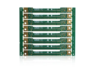
Optical-module interfaces
The separate optical solution page lists POFV, long/short and graded gold fingers, and blind/buried holes. It publishes 5–7% impedance tolerance, 50 μm moulding tolerance and ±30 μm gold-finger dimensions, without tying them to this photographed panel.
Ask for: the drawing dimension controlled by each tolerance, datum scheme, connector plating specification, via fill/cap method and impedance coupon/report for the approved stack.
A named optical-module application does not establish an assembled optical module, a qualified data rate or loss performance. Welgao’s manufacturing examples here are circuit boards.
A sample route is not the volume-production specification.
The current process page separates Batch from Sample. The following rows are reproduced by their actual column position in the rendered table; they are not a combined promise for either catalogue photograph.
| Condition | Batch | Sample |
|---|---|---|
| Layers | ≤32 | 46 |
| Finished thickness | 0.30–3.2 mm | 3.5 mm |
| Inner-layer thickness minimum, T/T | 0.063 mm | 0.05 mm |
| Interlayer alignment | ±63 μm | ±50 μm |
| Finished outer line / space | ≥63 / ≥63 μm | 50 / 50 μm |
| Finished inner line / space | ≥50 / ≥50 μm | 38 / 38 μm |
| Mechanical drill minimum | 6 mil | 4 mil |
| Green solder dam width | >3 mil | 2.5 mil |
| Other-colour solder dam | >4 mil | 3.5 mil |
Specify whether your design needs a sample run or a repeatable volume route, and obtain a written rule set for the chosen copper and laminate. A mechanical drill minimum is not a finished-hole minimum after plating.
Rows that need an engineering clarification
The batch impedance row, for line width below 89 μm, literally reads “≥±7%”; the sample column reads ±5%. The separate optical solution uses 5–7%. These do not establish one universal ±5% production capability.
The batch drill-to-pattern 4L row reads ≥24.5 mil, while 6L–14L reads ≥5.5 mil; the microvia annular-ring row reads ≥23.5 mil. Two through-hole-copper rows share the same line-spacing condition and print ≤25 μm / ≤20 μm. We do not silently reverse signs, remove digits or turn ambiguous units into selectable limits. Request a revised drawing rule and the finished plating acceptance definition.
Release the copper stack before approving the small geometry.
Welgao’s thick-copper solution describes ≥3 oz boards, a special lamination programme, etching commonly performed twice, and special resin-filling treatment at 8 oz and above. These are process statements, not the copper weight of the pictured power panel or proof that the finest routing row applies at 8 oz.
Planar-transformer circuit
The planar solution names 2–6 oz copper and control of coil-width consistency, total board thickness and dielectric uniformity. Supply the winding geometry and connections, layer-by-layer copper, insulation build and the electrical/mechanical acceptance requirements. Its generic transformer efficiency and frequency discussion is not a measured performance report for a PCB example.
High-current multilayer board
Define the finished copper requirement and allowable variation at the narrowest current path, the balance between inner and outer copper, material grade and board-flatness limit. Ask which lamination and filling steps are proposed, and what cross-section evidence will be delivered.
The 2025 annual report discusses 30-layer DC-DC technology and introduction of embedded copper, resistance and capacitance processes. That dated technical disclosure is separate from the website’s batch/sample table and does not supply a complete approved construction for your order.
Put the plant on the quotation and the release sheet.
The issuer’s 2025 annual report distinguishes three manufacturing bases. This is a more recent operational account than the About page’s forward-looking Thailand opening wording; it describes the reporting period, not today’s available capacity.
- HUIZHOU
Samples, small batches and product variety
Annual-report positioning includes thick copper and higher-value products. The website gives No.116 Jianshe Road, Longyuan Industrial Park, Mabei Town, Boluo County. Confirm which trial process will transfer to the production lot and whether another site needs qualification.
- JI’AN, JIANGXI
Medium and large production batches
The report describes automated and digitised production lines. The registered address and website business address are No.1 Yongjin Avenue, Jinggangshan Economic and Technological Development Zone. An engineering approval should name this plant when the quotation proposes volume production here.
- AYUTTHAYA, THAILAND
A Southeast Asian manufacturing base
The annual report states the Thailand factory had entered production. The website contact address is 86 Village M.4, Nong Nam Som, Uthai, Phra Nakhon Si Ayutthaya 13210. Confirm the actual contracting entity, approved site process and shipment origin; a group capability is not automatically transferable to Thailand.
The issuer’s office is separately listed at room 1004, 10th floor, Huipeng Building, No.5 Qihutang Road, Huizhou. An office address is not a fabrication location. The website separates Jiangxi, Huizhou and Thailand business departments; choose the right department for the proposed route rather than assuming every quote comes from Ji’an.
Specify what the shipment evidence must contain.
The annual report describes order review followed by engineering/sample development for new products, production planning and shipment inspection. It explicitly permits approved outside processing when a process cannot meet the production plan. Ask which steps will occur at the named site and which approved subcontractors, if any, will be used.
It also describes copper-thickness, impedance and thermal-shock sampling before shipment. Sampling does not mean every finished board receives every test. Put the lot definition, sample size, acceptance criteria and report format in the quality agreement.
The workshop gallery labels drilling, lead-free HASL, lamination, outer-layer inspection, LDI exposure, electrical test and shipping. It does not identify a complete brand/model/quantity inventory or attribute every photograph to a specific site. The labels are useful process context; the actual equipment and test coverage for your design still belong in the fabrication review.
Make the first inquiry actionable.
Include fabrication files and revision, selected site and sample/volume plan, copper and material stack, critical drawing dimensions, via fill/cap requirements, electrical acceptance and required shipment reports. Request one approved drawing-rule sheet against those inputs. For an optical connector, include the mating interface and contact finish; for a power board, include dielectric and current-path requirements.
Prepare the engineering RFQ →Sources behind this profile
Individually researched on 8 October 2026. Original catalogue images are application examples with unspecified individual stacks. Website process statements and dated issuer disclosures remain separate; neither is a PCBVerified factory certification.
- MANUFACTURER / IDENTITYCompany profile and product families ↗
- ISSUER / 2025 REPORTLegal identity (p6), outside processing and sampling (p10), site roles (p13) ↗
- MANUFACTURER / POWER EXAMPLEPower supply, new energy catalogue panel and original image ↗
- MANUFACTURER / OPTICAL EXAMPLEOptical module catalogue panel and original image ↗
- MANUFACTURER / PROCESSRendered Batch / Sample columns and literal ambiguous rows ↗
- MANUFACTURER / THICK COPPEREtching, lamination and 8oz resin-fill statement ↗
- MANUFACTURER / PLANARCopper and coil/dielectric consistency considerations ↗
- MANUFACTURER / OPTICAL PROCESSGold-finger, POFV, moulding and impedance statements ↗
- MANUFACTURER / WORKSHOPPublished process labels ↗
- MANUFACTURER / CONTACTThree business departments and separate office address ↗