

A portfolio centred on dense interconnects
Victory Giant Technology describes its business as research, development, production and sale of precision PCBs, with particular emphasis on HDI and high-layer multilayer boards. Its English site organizes the applications around AI/high-performance computing, smart devices, automotive electronics, telecommunications, medical devices and industrial uses.
The 2025 annual report on CNINFO identifies the issuer as 胜宏科技(惠州)股份有限公司, with its registered and office address in Huiyang, Huizhou. This cross-check concerns corporate identity, not validation of a proposed PCB build. That portfolio is useful for deciding whether to begin a technical discussion. It does not assign every published process to the same product, plant or release stage. The most informative source for the directory is the process page's explicit distinction between mass production and R&D.
28 layers describes a particular build-up.
The manufacturer describes 28-layer HDI mass production using 8+12+8, and 30-layer HDI R&D validation using 10+10+10. Both add up to their stated layer counts, but the numerical similarity does not make them interchangeable process routes. Send the intended via-stack and layer construction so engineering can compare the actual design with the disclosed structure.
The public page associates these technologies with AI acceleration cards. That is an application statement from the manufacturer, not evidence that a reader's accelerator design has already been qualified.
70+ layer production is not a 70-layer HDI promise.
The same page states mass-production capability for 70+ layer multilayer PCBs and technical capability for 100+ layer multilayer PCBs. It associates that family with next-generation AI servers. Keep these multilayer claims separate from the 28/30-layer HDI build-ups.
| 28-layer HDI | Mass production; 8+12+8 |
|---|---|
| 30-layer HDI | R&D validation; 10+10+10 |
| 70+ layer MLPCB | Mass-production capability |
| 100+ layer MLPCB | Technical capability |
“70+” is not an exact upper ceiling. Nor does the table supply a common line/space, drill, thickness and impedance envelope for all four routes. Obtain a current construction-specific capability response for those requirements rather than inferring them from layer count.
Ask how the build will be inspected.
Victory Giant’s production gallery names LDI exposure, high-precision CCD back drilling, back-drilling CT examination, ATG flying-needle testing and vacuum resin plugging. These are manufacturer equipment listings. The entries do not assign a plant, machine count or calibration record to your proposed build.
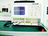
Define the electrical result, not just the instrument.
The testing gallery names impedance testing, a central laboratory, TG testing and metallographic microscopy. For your RFQ, specify target impedance, coupon construction, tolerance and the delivered record. A historic photograph is not evidence of the current calibration or the finished board’s tolerance.
Agree any channel-loss or reliability acceptance separately. The public gallery does not provide those thresholds for the 28-layer HDI route.
Route different projects to different questions.
Signal path and construction
Provide laminate grade, reference layers, via stack and loss/impedance acceptance. Ask which disclosed manufacturing route supports the full build.
Qualification and change control
Specify environmental exposure, traceability and customer approval requirements. An application label does not establish your order's qualification.
The website also lists FPC in several application families. That product listing does not extend the rigid HDI build-up figures to flexible circuits. Define the selected family before comparing capabilities.
Put process maturity in the quotation.
- Send a complete constructionInclude layer sequence, build-up, via connectivity, finished thickness, copper, laminate and high-speed acceptance requirements.
- Ask which released route appliesHave the manufacturer distinguish a mass-production route from a development or sample-validation route, and identify the production location.
- Agree the step from sample to volumeRequest the qualification evidence, change-control rules and acceptance reports needed before repeating the build at the intended lot size.
Start with PCB business, then name the fabrication site.
The official contact page gives the headquarters at Hangcheng Technology Park, Danshui sub-district, Huiyang District, Huizhou, and a separate PCB business contact. It also publishes US, Japan and European business contacts; those commercial addresses do not establish additional fabrication locations.
Sources behind this profile
Official sources checked on 8 October 2026. Production and technical-capability descriptions remain manufacturer statements; no independent process qualification or combined-limit guarantee is inferred.
- MANUFACTURER / PORTFOLIOCompany introduction and application families ↗
- MANUFACTURER / PROCESSHDI mass-production / R&D and MLPCB maturity labels ↗
- MANUFACTURER / EQUIPMENTProduction equipment names; image availability varies ↗
- MANUFACTURER / TESTINGTesting gallery and historic impedance-tester image ↗
- MANUFACTURER / CONTACTHeadquarters and separate PCB business contact ↗
- REGULATORY FILING / IDENTITY2025 annual report, company information on printed page 6 (PDF) ↗