Huizhou Trustwin Electronics Development Co., Ltd.
惠州市众信天成电子发展有限公司 · Guangdong
Official sources reviewed2026-10-08
HUIZHOU PRODUCTION / QIANHAI BUSINESS CONTACT
Trustwin's catalogue is strongest when you compare complete constructions.
Huizhou Trustwin Electronics Development Co., Ltd. is the English name on the manufacturer's company page and posted Huizhou quality-system documents. Its Chinese entity is 惠州市众信天成电子发展有限公司. The official contact page places manufacturing at Heshan Industrial Park in Yuanzhou, Boluo County, and separately names Qianhai Trustwin (Shenzhen) Technology Co., Ltd. at a Shenzhen office.
Its published examples span photovoltaic and energy storage, industrial control, automotive electronics, medical electronics, communications and LED displays. Eight detail pages provide much more useful purchasing information than those application labels alone: different copper weights, stack thicknesses, resin plugging, several impedance targets, cleanliness fields and depth-controlled machining.
These examples are manufacturer-published constructions. Select the closest one, then release the stack, material, process and acceptance requirements for your design. The photographs below are the full originals on the corresponding detail pages; their appearance is not used to invent specifications.
PHOTOVOLTAIC / ENERGY STORAGE CATALOGUE
Same copper headline, two different thicknesses.
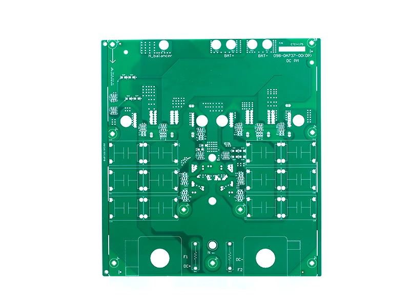
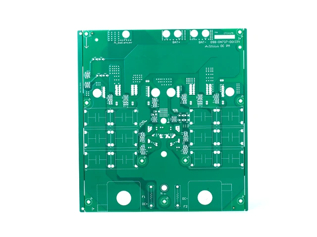
Product 34 · eight-layer TG thick copper plate.
Eight layers · 2.3 mm
Material and copper
TG170 · 3 oz inner / 3 oz outer
Published hole information
0.40 mm aperture · 5.7:1 aspect ratio · 25 µm hole copper
Finish and process
“Tin deposition” · press-fit / crimping-hole process
Ionic contamination field
≤1.0 µg Eq NaCl/cm²
The source does not identify whether the 3 oz refers to starting or accepted finished copper. Specify copper by layer, press-fit hole diameter and tolerance, hole-wall plating and the connector's fit requirements. Confirm the actual tin finish process and its assembly acceptance.
0.40 mm aperture · 7.2:1 aspect ratio · 25 µm hole copper
Finish and process
“Tin deposition” · press-fit / crimping-hole process
Ionic contamination field
≤1.0 µg Eq NaCl/cm²
The extra layers and thickness change the construction even though the copper and aperture fields look similar. Agree lamination, dimensional tolerance and cross-section sampling for the ten-layer build. Do not substitute the eight-layer stack without a released engineering change.
INDUSTRIAL CONTROL / MEDICAL CATEGORY
High layer count needs a net-class and interconnect brief.
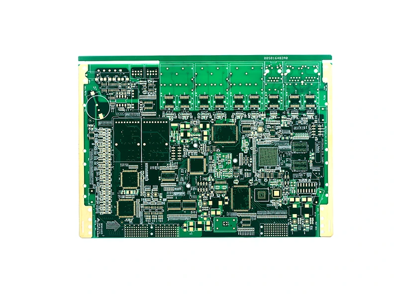
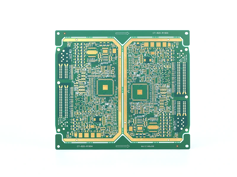
Product 18 · 26-layer TG resin-plug-hole board.
26 layers: vacuum resin plugging
The published construction is 4.2 mm, TG170, 1 oz inner and outer copper, 4 mil minimum line width and immersion gold. Its aperture field is 0.45 mm, with 25 µm hole copper and a stated 9:1 aspect ratio. The detail also names vacuum resin plugging, a 0.3 mm minimum BGA diameter and seven impedance controls: three at 80 Ω and four at 100 Ω.
Supply the via-in-pad drawing, fill/cap requirements and BGA land definition. Clarify what “BGA diameter” measures before treating 0.3 mm as ball size, pitch or pad acceptance. For the seven controls, identify each net class, single-ended or differential interpretation, coupon structure and tolerance. No product-specific impedance tolerance is supplied.
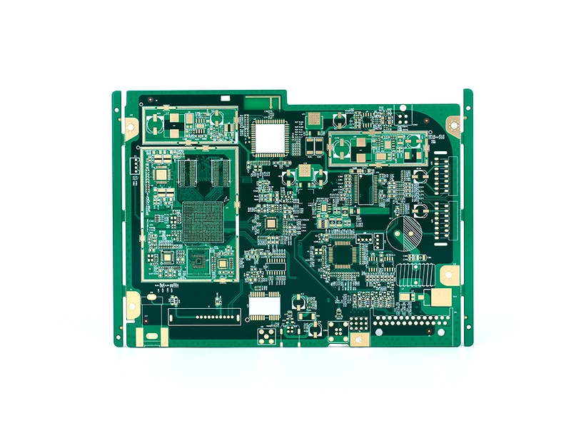
Product 39 · 28-layer board in the medical-electronics catalogue.
28 layers: eight impedance controls
This separate example specifies 4.2 mm, TG170, 1 oz inner and outer copper, 4 mil minimum line width and immersion gold. Its 0.40 mm aperture field and published 11:1 aspect ratio differ from product 18. The eight listed impedance controls are three 50 Ω, one 75 Ω, two 90 Ω and two 100 Ω.
“Medical electronics” is the manufacturer's application category. It does not establish a medical-device approval or qualification of this board for a particular use. Release the laminate grade, dielectric stack, test coverage and document retention needed for your equipment. The published aspect ratio is retained rather than recalculated into an accepted finished-hole specification.
Neither detail page gives minimum spacing or defines its aperture as a finished hole. Those fields remain unknown in the shortlist. The separate generic process window is useful for a first engineering conversation; it does not resolve these missing product-specific dimensions.
MACHINING FEATURES THAT NEED A REFERENCE SURFACE
Controlled-depth routing and controlled-depth drilling are different briefs.
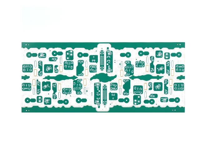
Product 21 · controlled-depth slots.
Blind routing + back drilling
4 layers · 3.0 mm · TG150 · 1 oz · immersion gold. The detail lists an 8 mil minimum line width, 0.30 mm aperture, 25 µm hole copper and 10:1 aspect ratio.
The source names the operations without specifying cavity depth or remaining stub. Mark the reference face, depth tolerances, keep-outs, residual dielectric and residual stub on the fabrication drawing. Identify which features receive each operation and how they will be inspected.
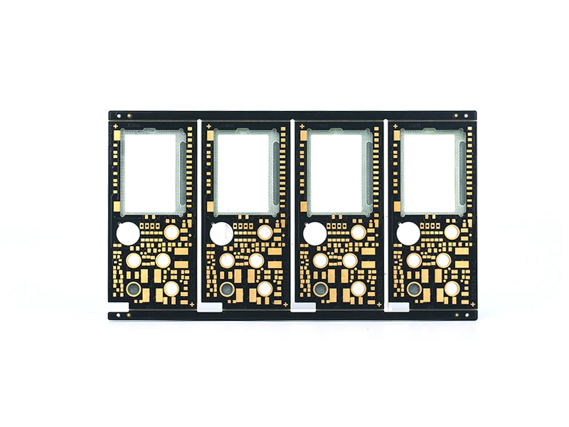
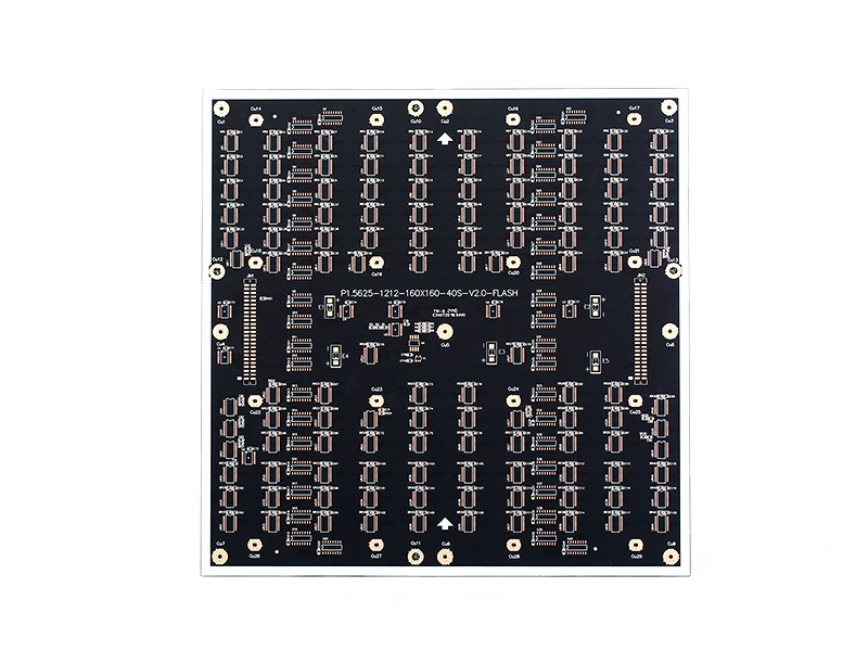
Product 29 · LED controlled-depth drilling.
LED drill depth: 1.2 mm
4 layers · 2.0 mm · TG150 · 1 oz inner / outer · OSP. This example instead lists 4 mil minimum line width, a 0.20 mm aperture field, 20 µm hole copper and a 10:1 aspect ratio.
Its special notes say P1.5625 LED board, 1.2 mm controlled drilling depth and ink-colour control. Release depth from a named reference surface, its tolerance and inspection points. Agree the solder-mask colour standard and OSP handling/assembly window. LED pitch is not the trace-width limit.
TWO SIX-LAYER CONSTRUCTIONS / DIFFERENT ACCEPTANCE FIELDS
Cleanliness, halogen content and line tolerance belong in separate requirements.
Product 38 · automotive-electronics category.
Automotive: ionic contamination field
1.6 mm · TG170 · 1 oz inner / outer · immersion gold; 8 mil minimum line width, 0.40 mm aperture, 25 µm hole copper and 4:1 aspect ratio.
The individual limit is ≤0.75 µg Eq NaCl/cm². Agree the extraction/test method, normalization area, sampling and lot report. An ionic-contamination number and an IATF certificate are different evidence; neither establishes customer approval of your specific part.
Product 42 · communication-electronics category.
Communications: three-core construction
2.0 mm · halogen-free TG170 · 1 oz inner / outer · silver deposition; 8 mil minimum line width, 0.30 mm aperture, 25 µm hole copper and 6.6:1 published aspect ratio.
The source specifies a six-layer pressed structure using three core boards and ±10% line-width tolerance. This is not an impedance tolerance. Identify the laminate brand/grade and halogen declaration, copper/dielectric stack, silver finish and storage/assembly requirements.
OFFICIAL PROCESS SHEET / ROUTINE AND EXTREME COLUMNS
Use a manufacturing window with its conditions attached.
Routine column
Maximum 20 layers.
4 / 4 mil trace/space at 1 oz.
0.2 mm mechanical drill; stated thickness/hole ratio 10:1.
Maximum processing size 600 × 710 mm; outline tolerance ±0.127 mm.
Extreme column
Maximum 28 layers.
3 / 3 mil trace/space at 1 oz.
0.15 mm mechanical drill; stated ratio 16:1.
420 µm outer copper; 210 µm inner copper.
Maximum processing size 600 × 800 mm; outline tolerance ±0.05 mm.
Thickness, impedance and the 30-layer discrepancy
The common thickness range is 0.4–5.0 mm. Thickness tolerance is ±0.1 mm at ≤1.0 mm and ±10% above 1.0 mm. The impedance row distinguishes ≤50 Ω: ±5 Ω from >50 Ω: ±10%; the first is an absolute resistance window, not a universal ±5% claim.
The China Power Supply Society member introduction describes 2–30-layer work, while the manufacturer's process sheet says routine 20 and extreme 28 layers. The association introduction is member-supplied company information, not a factory audit. A 30-layer order needs a current engineering-approved construction and process route; this page does not turn that description into an accepted combined capability.
The sheet also lists FR-4, high-Tg halogen-free material, metal substrates, high-frequency material and FPC; its special-board row mentions first-order HDI, buried holes, controlled impedance, high-frequency/FR-4 hybrid pressing and copper-base boards. No corresponding laminate grade, flexible construction or laser-drilling model is inferred for the eight rigid examples above.
What the factory tour actually shows
The official tour captions one photograph “Electroplating line” and seven others “Testing equipment”. The images provide a manufacturing view, but no complete asset register, machine model list, calibration dates or current utilization. Ask for the plating route and cross-section record for a heavy-copper or high-aspect-ratio order, and the named test method, fixture/netlist control and calibration records for electrical and impedance acceptance.
The company describes ERP coordination of procurement, staffing, production planning and delivery. Turn that general statement into an order-level commitment: agreed lead time, lot traceability, engineering revision control and change notification.
ENTITY MATCH / PRINTED SCOPE / CURRENT STATUS
Match the Huizhou factory, the sales contact and the released paperwork.
Identity and location
The manufacturing documents identify Huizhou Trustwin at Heshan Industrial Park, Yuanzhou, Boluo, with unified social credit code 914413225516813169 on the ISO copies. The Shenzhen office in the official contact page is at 8D Xinlikang Building, 3044 Xinghai Avenue, Qianhai, Nanshan, under a separately named Qianhai company. Match the contracting party, fabricating site and export documents before release.
The government-hosted Guangdong 2024 first-batch science-and-technology SME list includes the exact Chinese Huizhou entity on PDF page 358, entry 8936, number 2024441322A8008936. This is a historical registry entry, not a manufacturing-quality certificate. China Power Supply Society's first-party directory lists it as member 2483, joined 15 June 2026, with the same Heshan location and trustwin-pcb.com website.
The society's company introduction states establishment in March 2010, a 26,000 m² production site and 60,000 m² monthly output. Those are company-provided figures, not audited available capacity. The manufacturer page separately says 16+ production years; a homepage reference to 30+ years of experience is not used as the company's establishment date.
The visible official business address is sales@trustwin-pcb.com. The footer's email link points to a different named address, teresa.yu@trustwin-pcb.com. Confirm the intended order contact through an established business channel. No email or deliverability test was sent during this research.
Individually researched 8 October 2026. Eight product detail pages and original images, the full process-sheet image, factory tour, posted document copies and primary identity records were read separately. Product-specific gaps, source conflicts and document scope are retained rather than merged into a stronger specification.