Motherboards, network boards and contact-edge cards need different release drawings.
Shenzhen Trustech Electronics, 深圳全成信电子有限公司, describes its core business as two- to twelve-layer printed circuit boards for motherboards, graphics and expansion cards, networking, telecommunications, servers and workstations. The company history dates establishment to June 2002, trial production to April 2003 and volume shipments to June 2003. The official Shenzhen address is Jiaotang Western Industrial Zone, Xihuan Road, Shajing, Bao’an.
For a buyer, its catalogue is useful because the examples identify the application and surface treatment. The separate technical table describes fabrication limits. These are two different kinds of information: an OSP motherboard photograph does not, by itself, establish the board’s layer count, line width or approved electrical stack.
Manufacturer’s original company-page photograph. It is not a dated independent site inspection.
Specify where the finish is required and what the board must mate with.
The following images come from four corresponding product pages, each dated 28 September 2018. Their stated finishes are retained. The photographs are catalogue examples, rather than current stock models or dimensioned fabrication drawings.
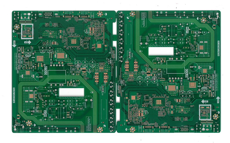
Entry titled networking / OSP; its use field says industrial electronics.
Networking / industrial board · OSP
The entry names OSP, but does not state a link rate, substrate grade or impedance target. Send the stack, differential and single-ended impedance groups, reference planes and coupon drawing. For connectors and mechanical interfaces, specify finished-hole dimensions and pin tolerances separately from drill tooling.
Ask which OSP process, storage conditions and solderability acceptance apply to the delivery interval. A networking label does not establish low-loss laminate or a tested high-speed channel.
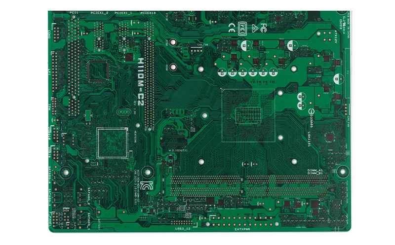
Official motherboard / OSP entry. Layer count and board thickness are unstated.
Motherboard · OSP
Release connector and mounting datums together with the copper and dielectric stack. Separate socket-area flatness, finished-board thickness and hole fit from global dimensions. The official table gives a general bow/twist figure; agree the actual acceptance and measurement state required by the assembly process.
Identify whether the order is bare PCB manufacture or a populated assembly. This catalogue describes a PCB; it does not establish component procurement, assembly testing or motherboard platform compatibility.
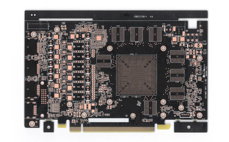
The website retains the notation “G/F” without defining its plating thickness. Specify the contact-edge plating stack, nickel and gold thickness, contact dimensions, bevel and exclusion zones on the drawing. Do not turn the finish abbreviation into an assumed hard-gold thickness or insertion-cycle rating.
Approve how the solderable and contact areas are separated, then inspect the first article against the same edge datum and connector drawing. Define copper balance and finished thickness where card stiffness or socket fit is critical.
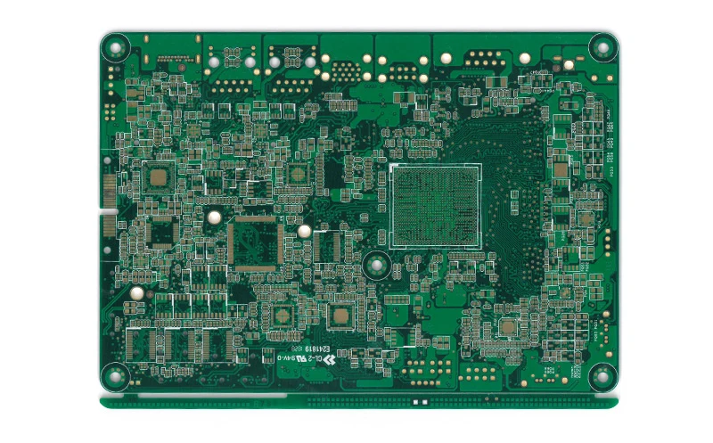
Consumer electronics; the source specifies chemical nickel/gold.
Consumer-electronics PCB · chemical nickel/gold
The entry calls the treatment 化学镍金 / 化金. It supplies no coating thickness, chemistry specification or pad-flatness result. Put the required finish standard, thickness and test acceptance in the fabrication package instead of treating the photograph as a finish certificate.
For fine-pitch assembly, agree solder-mask registration, exposed-pad dimensions and acceptable repairs. Keep material substitution, finish substitution and process requalification subject to written approval.
TECHNICAL TABLE / DRAWING REVIEW
Use the published limits to check the whole construction.
Routing and stack
Layer range
2–12
Finished board thickness
0.4–2.5 mm
Minimum line / space
3 / 3 mil; source also gives 0.08 / 0.08 mm
Layer registration
±2 mil; source gives ±0.05 mm
Working panel
10 × 10 to 20 × 24 inches
Holes and plating
Minimum finished hole
0.20 mm
Published drill range
0.2–6.5 mm
Plating aspect ratio
7:1
Minimum plated hole copper
0.020 mm
Hole-diameter tolerances as labelled
Drilling: PTH ±0.08 mm; NPTH ±0.05 mm
The manufacturer prints rounded metric equivalents alongside mil values. Keep the intended unit and acceptance limit explicit on the drawing. Its tolerance row is headed drilling diameter: do not silently reinterpret it as a finished press-fit hole tolerance. Likewise, a 0.20 mm finished hole and a 2.5 mm thick board should not be assumed to meet the separate 7:1 plating limit together. Ask engineering to approve the proposed hole structure and plating route.
Impedance needs a target and an agreed range.
The source prints “±8–15%ohm” for impedance control. This profile preserves that wording as a manufacturer-reported range and does not reduce it to a universal ±8% promise. Send nominal impedance, tolerance, reference planes, stack, copper and coupon geometry. Ask which value applies to the proposed construction, how it is measured and which records accompany delivery.
The same table states ±0.10 mm finished-board thickness tolerance, ±0.10 mm outline tolerance and bow/twist below 0.7%. Define the inspection method and local critical features where a global limit does not resolve connector fit or assembly requirements.
PROCESS CONTROL / REPEAT SUPPLY
Ask for a traceable fabrication lot, not only a passing sample.
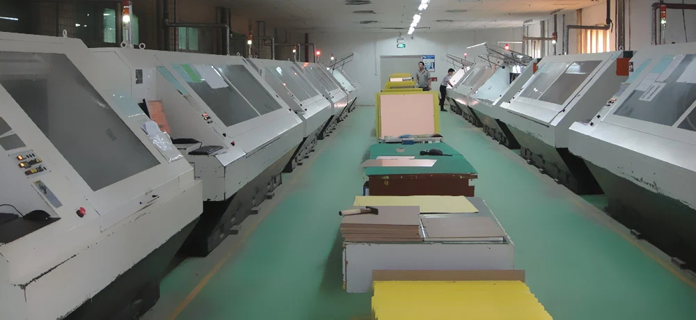
Manufacturer equipment-gallery original. No equipment model, calibration status or present availability is inferred from this photograph.
Trustech publishes a quality-control diagram covering incoming inspection, instrument calibration and measurement-system analysis, statistical process control, nonconforming-product handling and traceability. Its traceability section links material, lot number, date code, mould, shift, operator and surface code to production and sample records. These are useful topics for the purchase record; the diagram is not a demonstration that a particular order has followed each control.
Agree the evidence delivered with the lot
Request the approved laminate and bonding-sheet grades, supplier and lot references, released fabrication revision, electrical-test coverage and agreed impedance coupon results. Specify how a failed coupon or dimensional result is segregated, investigated and reported. For a repeat order, require notification before material, finish, plant or critical process changes.
The equipment gallery supplies production photographs but no readable, complete machine register with capacities and calibration records. If a named imaging, drilling or measurement route is necessary for the design, obtain its process assignment and relevant capability record. Avoid assuming laser microvias or HDI qualification from the presence of general production equipment.
MANUFACTURING ENTITY / RELEASE CHECK
Keep the Shenzhen order and other group sites distinct.
The official history names the establishment of Hubei Trustech in October 2018. A later public notice includes Shenzhen, Hubei and Vietnam entities; the Hubei cleaner-production disclosure names Xiaochang’s Chengnan Industrial Park. These records do not identify which site will manufacture this buyer’s board. Obtain the invoicing entity, fabrication address and shipment address before approving the production route.
Shenzhen’s emergency-management department reported a visit to Trustech’s PCB electroplating workshop and wastewater-treatment pool in March 2023, in a notice published 3 April 2023. This provides a dated government record of those Shenzhen activities. It is a safety-management inspection report, not an endorsement of PCB quality, a current environmental permit or an independent capability certification.
Request replacement copies for a current qualification package.
The manufacturer-hosted ISO 9001 certificate AN23Q3020R4L names 深圳全成信电子有限公司 and manufacture of double-sided and multilayer PCBs up to twelve layers; its displayed validity ends 11 April 2026. The ISO 14001 copy AN23E2021R4L ends 20 April 2026. The displayed IATF 16949 copy 0424734 / 2021A669 covers PCB manufacture excluding product design and ends 12 September 2024. These dates precede this review, so the copies are historical evidence rather than active certification badges.
Ask for current issuer records covering the actual production site and scope. The catalogue also contains CQC construction documents, hazardous-substance process, energy, greenhouse-gas and RBA records; none substitutes for the exact material construction and qualifications required by an individual order. No current UL file ownership is established here.
One drawing, one plant, one acceptance record
Before production, reconcile the layer stack, hole structure and plating ratio, finish map, mechanical datums and inspection criteria. Use the corresponding application above to select a fabrication enquiry, then obtain written engineering approval for the combined construction. Retain first-article results and the agreed change-control procedure for recurring supply.
SOURCE TRAIL
Sources behind this profile
Individually reviewed 8 October 2026. Product examples, general process limits, displayed document copies and the dated government inspection record are separate sources. No current factory audit or active issuer certification is implied.