TOPSTAR CIRCUIT / THE BOARD ROUTE AND THE PRODUCTION INSTRUCTION
Start with the contact, the thermal stack or the signal stack.
Dongguan City Topstar Circuit Co., Ltd. · 东莞市鼎新电路有限公司 describes a business established in September 2011 manufacturing double-sided, multilayer and aluminium-base PCBs. Its catalogue is particularly useful for comparing connector interfaces, industrial half holes, thick-copper power boards and communications designs.
The official company page says samples and volume orders have their own manufacturing instructions (MI). This is the central sourcing question: what stays the same when the prototype is released for production, and what changes require approval?
We individually examined 56 catalogue pages and their corresponding original images, then selected 12 examples to cover distinct buying decisions. Similar catalogue photos are not extra suppliers, and general chart values are not added to examples that publish no individual specification.
CONTACTS, CASTELLATED EDGES AND TOOLING
Release the edge detail as carefully as the electrical netlist.
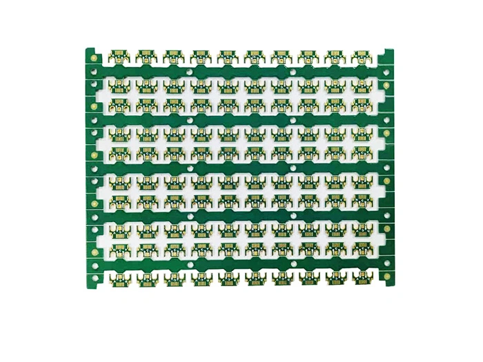
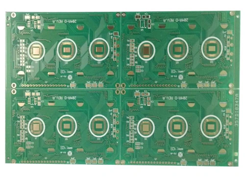
Topstar shows both single- and double-sided connector boards and a separately titled multilayer half-hole board. Their images provide manufacturing examples; none defines mating cycles, contact resistance or nickel/gold thickness.
Double-sided connector-board example
Layer title
Double-sided
Contact finish
No nickel/gold thickness or contact life specification
Provide mating contact, finish thickness, chamfer angle and edge datum. Do not treat a gold-coloured photograph as evidence of a hard-gold plating specification.
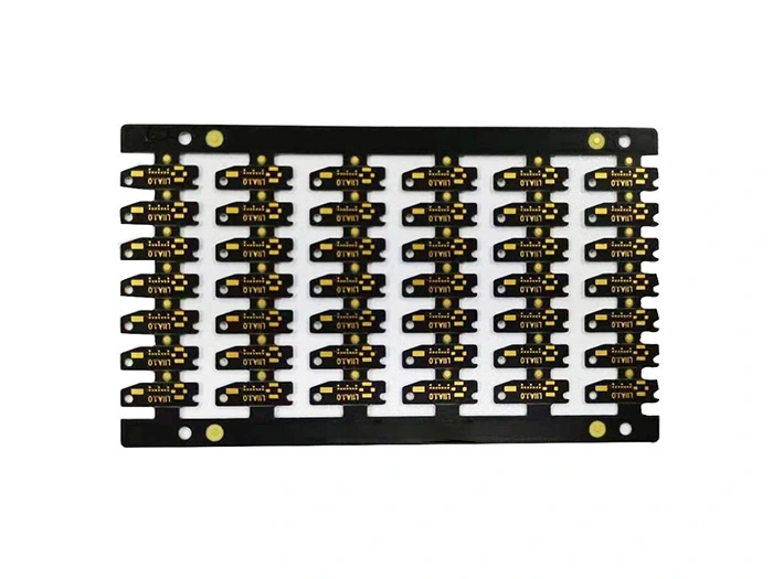
Single-sided connector-board example
Layer title
Single-sided
Contact geometry
No released dimensions or plating class
State contact resistance and insertion cycles, panel routing and solder-mask keep-out. Identify which contact surfaces require a wear-resistant finish.
Multilayer half-hole industrial board
Source title
Multilayer industrial board with half holes
Edge detail
Half-hole diameter and plating not stated for this example
Dimension the castellated edge, minimum remaining copper and burr criteria. Agree plating continuity and panel separation after soldering to a host board.
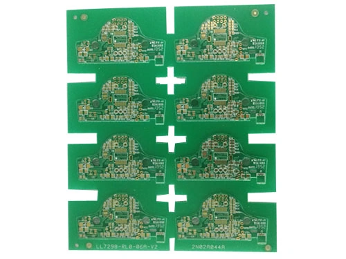
Compound-die punched board example
Manufacturing title
Compound-die punching
Tooling data
Tolerance, tooling cost and panel yield not specified
Ask which outlines and holes are punched together, tool maintenance, edge damage and first-article dimensions. Agree the tool ownership and changes from prototype routing.
POWER / CIRCUIT COPPER IS DIFFERENT FROM THE METAL BASE
Keep current-carrying copper and the thermal dielectric separate.
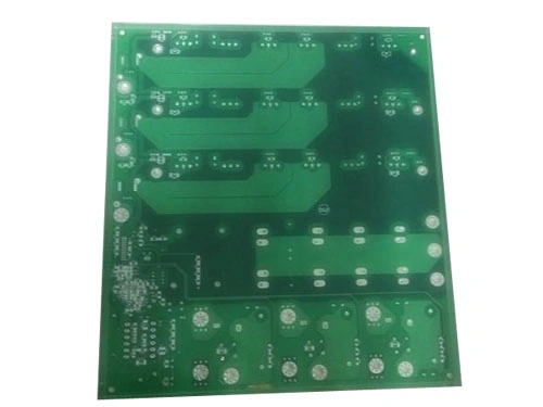
FR-4 TG150 thick-copper power board
Material title
FR-4 TG150
Copper wording
Thick copper; no finished oz value
Ratings
No instance-specific current or operating voltage
Set starting and finished copper, etch spacing and allowed temperature rise. Confirm laminate grade and Tg method; TG150 in the title is not a complete material certificate.
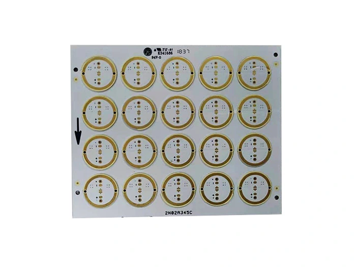
Double-sided aluminium-base board
Construction title
Double-sided aluminium-base board
Thermal stack
Dielectric grade, thickness and conductivity not specified
Define electrical connections between faces, isolation from the aluminium base and mounting interface. Request the metal/dielectric/copper section; the general FR-4 table is not an aluminium-board specification.
For the FR-4 power route
The title explicitly says FR-4 TG150 and thick copper, but supplies no copper weight. Define starting foil versus finished copper, etch spacing, vias and temperature rise. Request the laminate grade and thermal/reflow data for the selected stack.
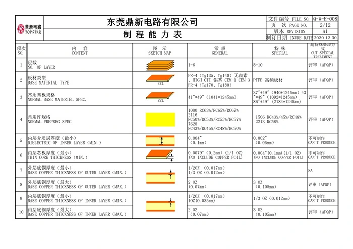
The general dated chart's conventional 2 oz and special 3 oz base foil maxima are separate rows for inner/outer copper. They are not finished-copper specifications of this power-board example.
For the aluminium route
Define base thickness, dielectric thickness/thermal conductivity, isolation voltage and conductor-to-base connection. A double-sided title needs a cross-section explaining how the electrical sides connect and remain isolated from the aluminium.
The FR-4 drilling, laminate and thickness rows must not be transferred to an aluminium stack. Quote thermal measurements with their units and test configuration, including the intended heat-sink interface.
SIGNAL ROUTES / APPLICATION TITLE IS THE START OF A SPECIFICATION
Choose the stack before borrowing an impedance tolerance.
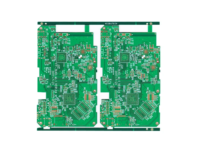
Four-layer rigid board example
Layer title
4 layers
Instance data
Thickness, finish, line/space and finished holes not specified
Release the four-layer stack, prepreg and impedance coupon. Choose the ordinary or special route using the dated chart rather than applying its smallest values automatically.
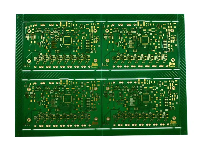
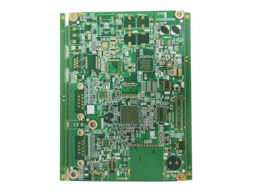
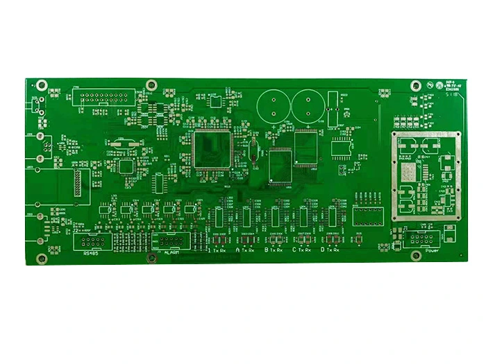
Multilayer communications mainboard
Application title
Communications mainboard
Stack
Multilayer; count not specified
Signal data
No instance-specific impedance or loss target
Supply actual signal rates, dielectric target and coupon method. A communications category does not establish RF laminate use or HDI build-up.
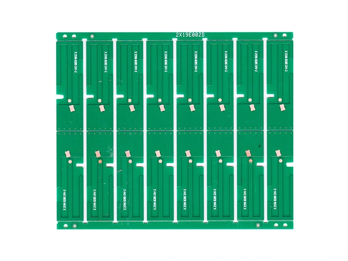
Antenna circuit-board example
Application title
Antenna circuit board
RF data
Frequency, Dk/Df and stack not specified
Ask for laminate grade, dielectric thickness and design frequency before comparing antenna loss or tuning. The catalogue image alone establishes none of these measurements.
FR-4 security-system board
Material title
FR-4
Application
Security electronics
Numeric limits
No board-specific layer, thickness or holes
State supply voltage, environmental conditions and connector loads. Agree the actual flame/laminate grade and acceptance record instead of quoting generic FR-4.
The homepage's impedance bands
Conventional
±3 Ω below 30 Ω; ±10% at or above 30 Ω.
Special
±3 Ω below 30 Ω; ±5% at or above 60 Ω.
Unspecified special band
The homepage does not state the 30–60 Ω special band.
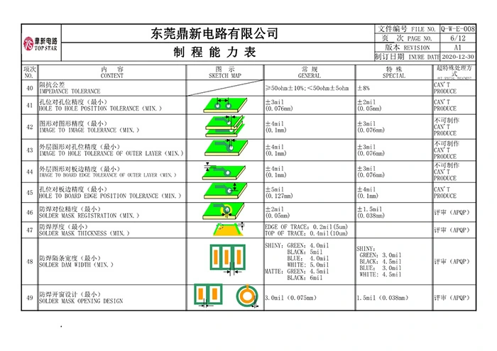
The dated table instead uses a 50 Ω boundary: conventional ±10% at/above 50 Ω and ±5 Ω below 50 Ω, with a special ±8% row. Confirm which revision governs the quote, single-ended/differential target, coupon, measurement method and acceptance band. There is no universal ±5% badge on this profile.
Medical-application circuit-board example
Catalogue family
Medical circuit boards
Approval scope
No device programme or regulatory approval supplied
Separate bare-board acceptance from the finished medical device. Specify lot traceability, cleanliness, reflow conditions and the device-specific supplier qualification.
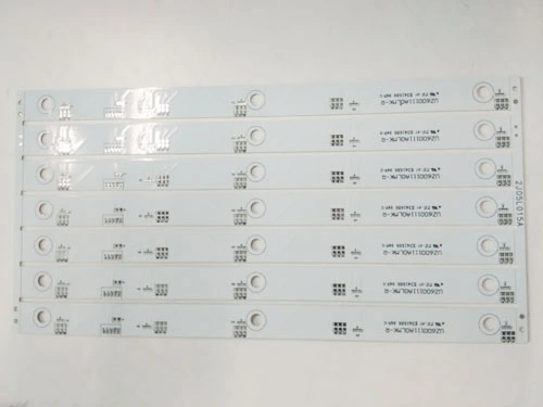
LED lighting/display board example
Application title
LED lighting and display
Base material
Not specified on this individual page
Identify the actual laminate/base rather than assuming every light-coloured LED board is aluminium. Supply thermal loss, solder-pad finish and dimensional mounting requirements.
Medical, automotive and LED application names are not approvals for a buyer's finished device. Supply the end-use environmental and traceability requirements, then agree a bare-board acceptance plan and the actual manufacturing entity.
2020-12-30 / REVISION A1 / GENERAL AND SPECIAL COLUMNS
A dated chart is a useful engineering reference, not a current combined promise.
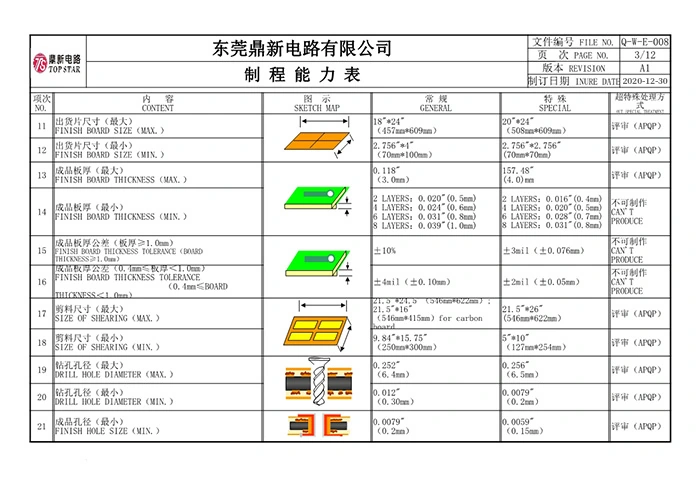
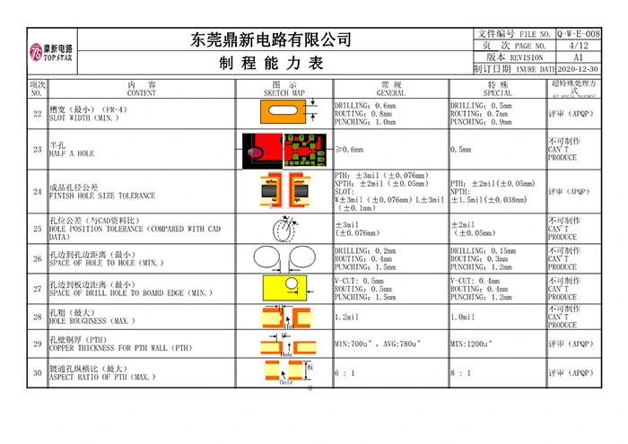
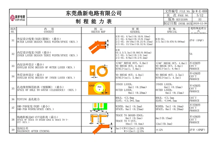
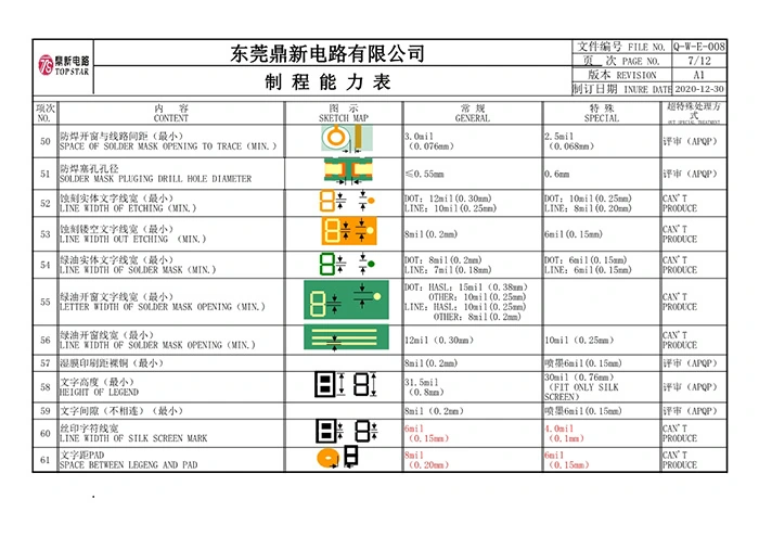
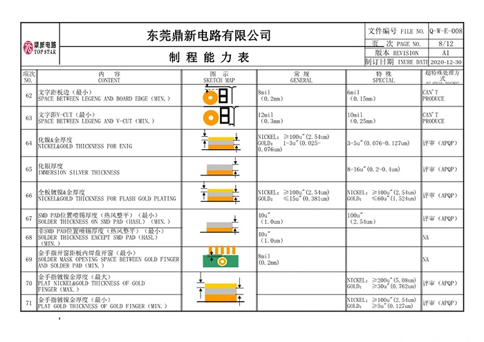
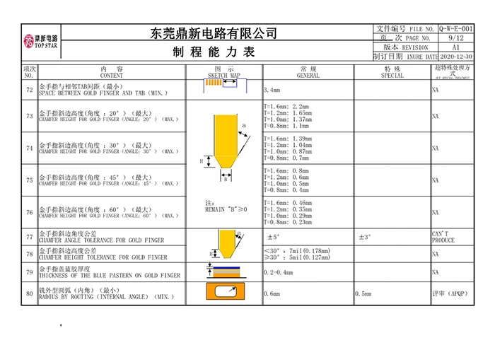
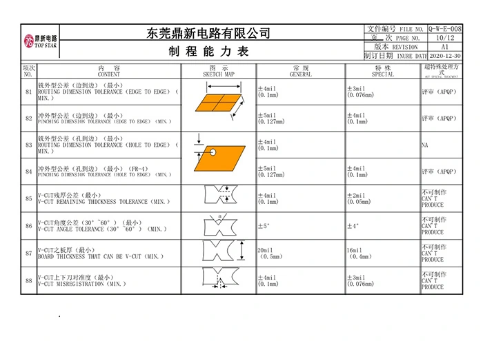
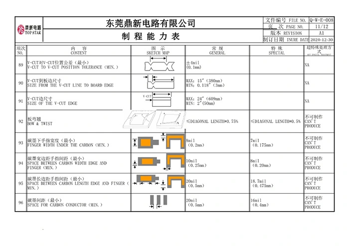
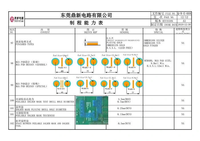
The original image table is dated 30 December 2020, revision A1. Most sheets show Q-W-F-008; the gold-finger sheet shows Q-W-F-001. The official homepage has separate undated claims including 0.2–8 mm board thickness and 3/3 mil line/space. Ask for the approved current revision when those figures differ.
The special finished-thickness row prints “157.48″” beside 4.0 mm; it is not a credible conversion and needs correction by the manufacturer. The outer-layer row also varies with copper weight: conventional 2 oz lists 10/10 mil and 3 oz 13/13 mil. This makes copper weight part of the route decision, not an independent filter.
Read the corresponding original process-table sheets
Original sheet 2/12, 30 December 2020. General and special columns retain their source scope.Original sheet 3/12, 30 December 2020. General and special columns retain their source scope.Original sheet 4/12, 30 December 2020. General and special columns retain their source scope.Original sheet 5/12, 30 December 2020. General and special columns retain their source scope.Original sheet 6/12, 30 December 2020. General and special columns retain their source scope.Original sheet 7/12, 30 December 2020. General and special columns retain their source scope.Original sheet 8/12, 30 December 2020. General and special columns retain their source scope.Original sheet 9/12, 30 December 2020. General and special columns retain their source scope.Original sheet 10/12, 30 December 2020. General and special columns retain their source scope.Original sheet 11/12, 30 December 2020. General and special columns retain their source scope.Original sheet 12/12, 30 December 2020. General and special columns retain their source scope.
MANUFACTURING INSTRUCTION / PROTOTYPE → REPEATABLE PRODUCTION
Use the first article to approve the route, not just a functioning sample.
Engineering release
Gerbers/netlist, stack and materials, critical edge drawing, finish and inspection plan.
Sample MI
Confirm actual construction, coupons, dimensional results and any special process.
Volume MI
Approve material/process changes, panel/tooling and the lot-linked release documents.
This sequence is a buyer's release checklist based on Topstar's separate-MI statement, not an audited production record. Agree how revisions are controlled, who approves substitutions and how the retained sample/MI is linked to the shipment.
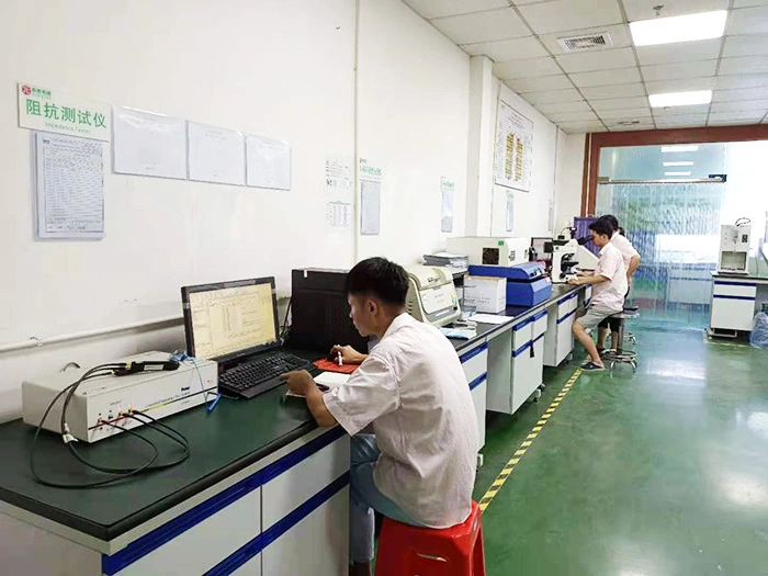
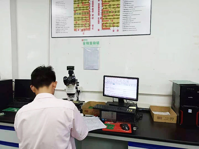
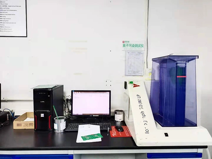
Manufacturer-labelled impedance tester — corresponding original gallery photograph.Manufacturer-labelled metallographic microscope — corresponding original gallery photograph.Manufacturer-labelled ionic-contamination instrument — corresponding original gallery photograph.
The homepage describes flying-probe and fixture testing. Request continuity/isolation results, impedance coupon reports where applicable, microsections and cleanliness conditions for the actual lot. A gallery photo establishes the manufacturer's published equipment description, not its calibration or the result of your board.
LEGAL ENTITY / SHIJIE CONTACT / DATED DOCUMENTS
Make the quoted plant and entity explicit.
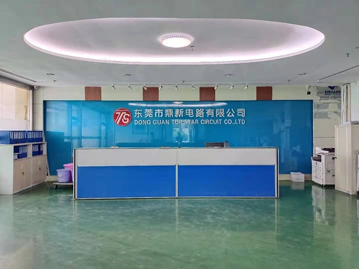
Original official company-gallery reception image.
The repeated footer has an extra digit in its telephone string; the two numbers here follow the dedicated contact page. The email has been read as an official contact source; no mailbox-control test or message was sent.
The undated company narrative gives 10,000 m², 26,000 m²/month and about 300 staff, and names a Hunan factory in its 2018 timeline. These do not establish current available capacity or allocate the pictured products to Hunan. Confirm where the order is made and which legal entity contracts it.
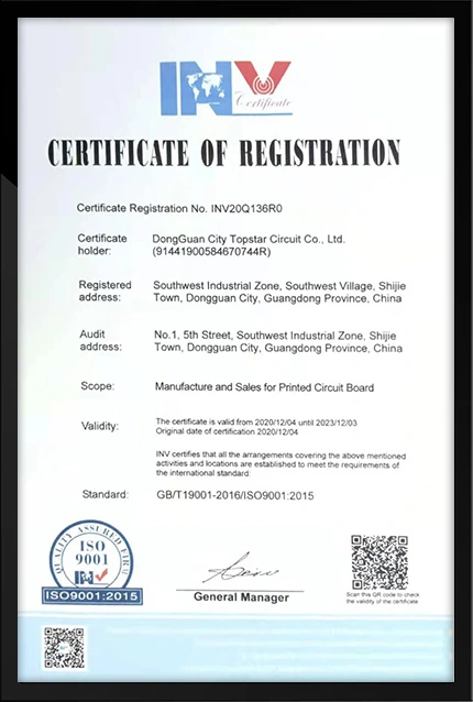
Historical certificate copies: validity and product scope
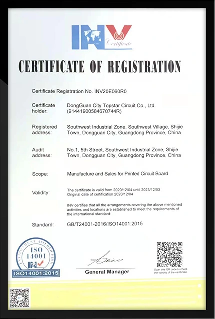
The INV ISO 9001 copy INV20Q136R0 and ISO 14001 copy INV20E060R0 name the Dongguan company and No. 1, 5th Street audit address. They cover PCB manufacture/sales and print validity 4 December 2020–3 December 2023.
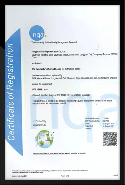
The NQA IATF copy T10934 / 0324160 covers circuit boards for instrument panels, excludes product design and expires 18 August 2021. Older 2008-standard ISO copies end on 30 November 2017. These historical copies are not current certification badges or approval of all applications.
Historical ISO 9001 copyHistorical ISO 14001 copyHistorical instrument-panel IATF copy
Obtain a renewed issuer record and actual plant/product scope before qualifying an order. The homepage's IPC Class III/GJB wording likewise requires an agreed standard edition and product acceptance plan.
SOURCE TRAIL
Sources behind this profile
Individually researched 9 October 2026: company and contact pages, 56 catalogue pages/original images, selected 12 distinct examples, full published process-table sheets and dated certificates. Homepage claims and dated chart columns remain separate; unknown example parameters are not inferred. Government-record retrieval attempts and source availability are recorded privately.