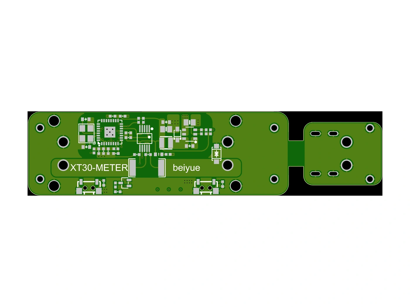
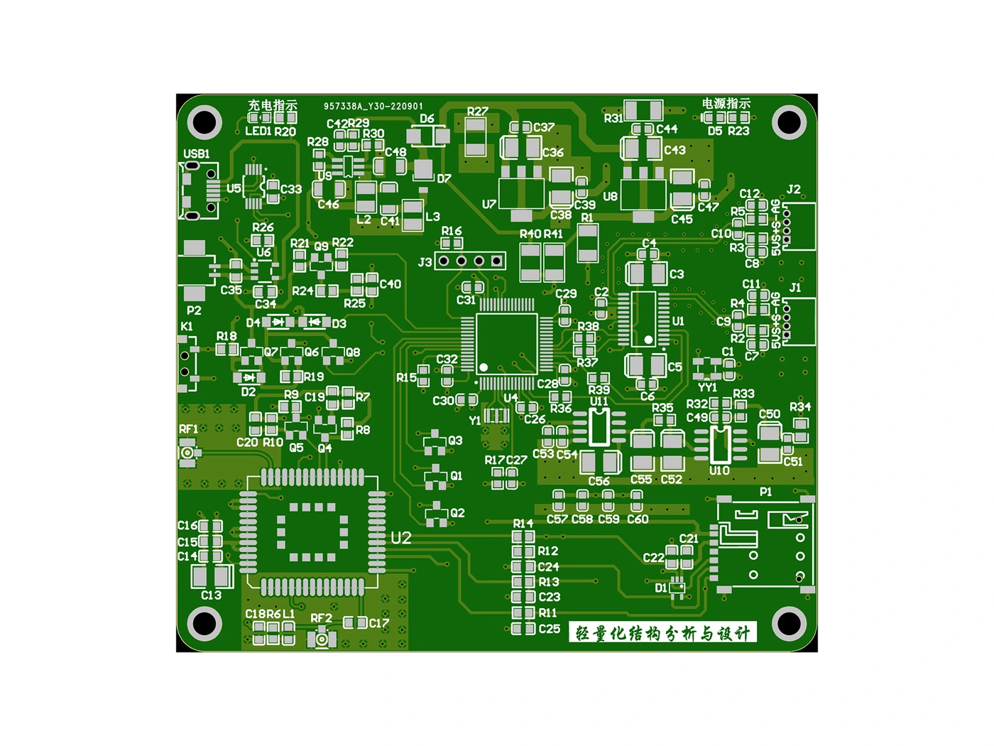
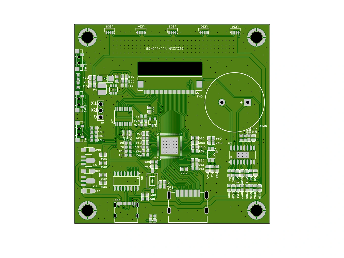
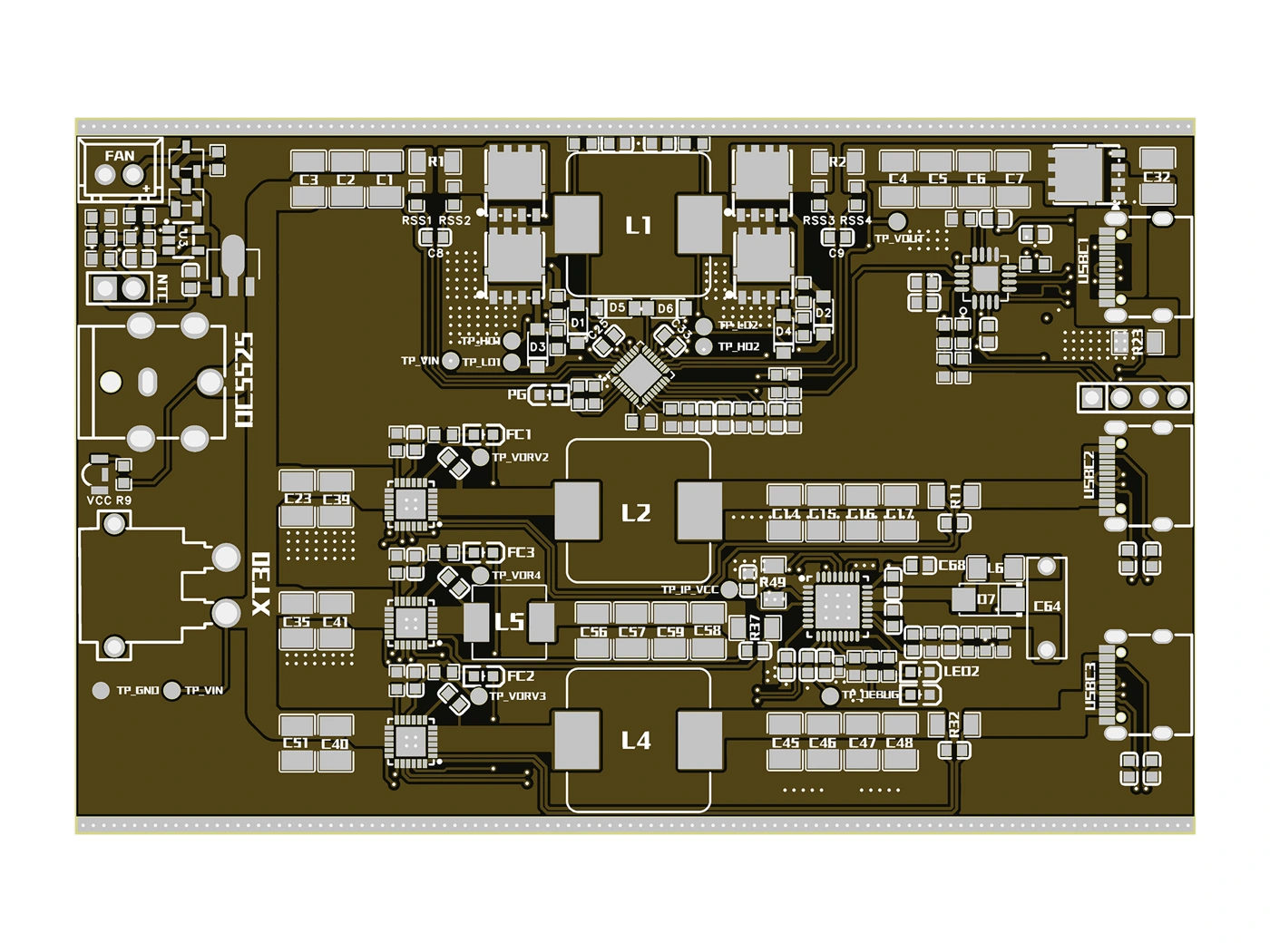
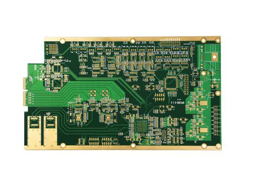
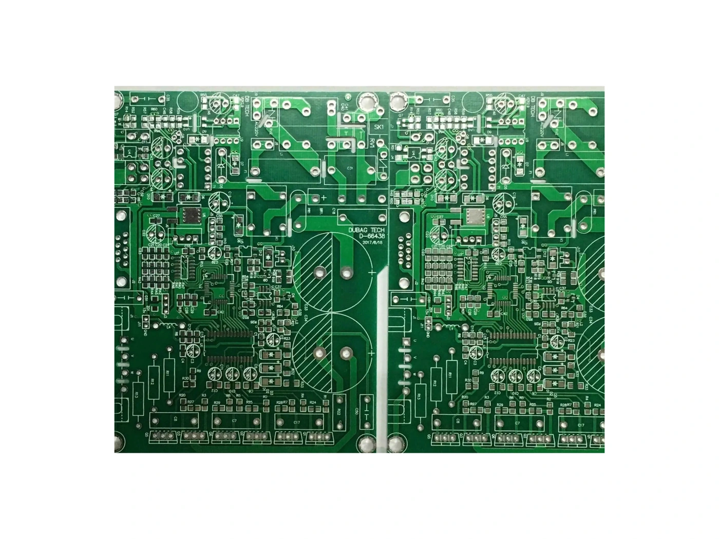
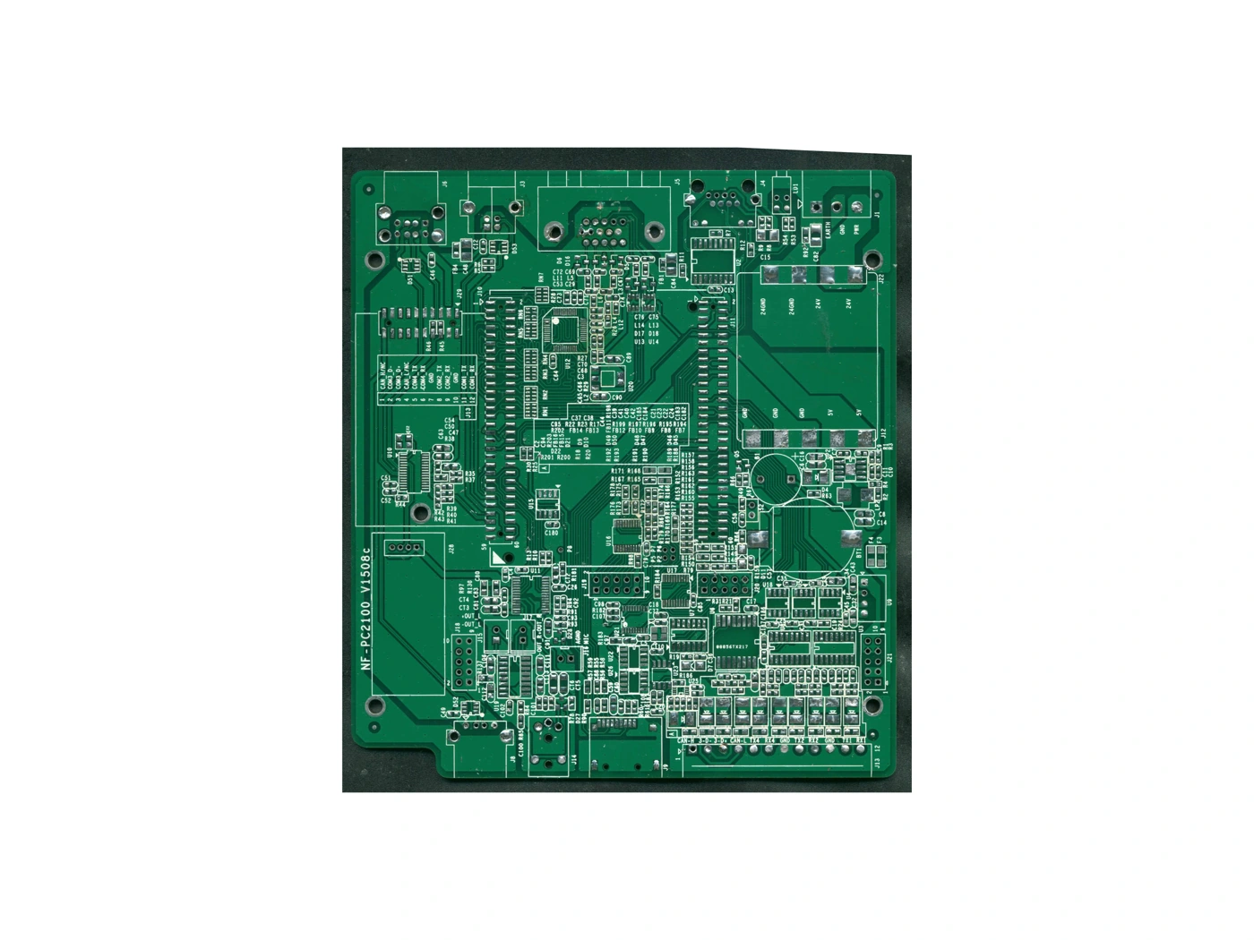
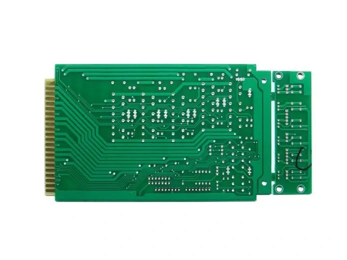
Keep the stackup tied to your drawing.
The individual titles explicitly supply four layers or a double-sided construction. Their descriptions otherwise explain what a PCB is; they do not provide a measured stackup, minimum line/space, copper thickness, finished hole or impedance tolerance. Only the explicit layer construction is available for numeric matching here.
For a four-layer board, specify the copper on each layer, dielectric and total thickness tolerances, via connectivity, registration and any impedance coupon. For a double-sided board, distinguish plated holes, non-plated holes and slots, and agree the electrical test file. Do not derive material grade from solder-mask colour or infer dimensions from a photograph.