REN CHUANG YI / FROM ENGINEERING LOT TO PRODUCTION
Start with the board's construction and the size of your order.
Shenzhen Ren Chuang Yi Electronic Co., Ltd. describes a business founded in 2000, initially providing solder-finish subcontracting, with full PCB-process production introduced in 2006. It now presents two manufacturing locations with different roles. The original Chinese legal name is 深圳市仁创艺电子有限公司; the Jiangxi base is identified separately as 江西仁创艺电子有限公司.
SHENZHEN / ENGINEERING & SPECIAL CONSTRUCTIONS
Rigid-flex, FPC, HDI and high-layer work
The company introduction places small and medium lots of 3–50 m² here. The address is Buildings 3 and 4, Jinfeng Industrial Zone, 45 Yonghe Road, Heping Community, Fuyong, Bao'an. The disclosed gallery shows lamination, drilling, plating, imaging, solder mask and electrical test stages.
JIUJIANG / REPEAT PRODUCTION
Conventional double-sided and multilayer boards
The introduction assigns medium and large lots of 100 m² or more to the Jiangxi base, in Chengxi Port Area, Jiujiang Economic and Technological Development Zone. The address page dates construction to 2020 and completion to early 2022. Ask which legal entity produces and invoices your order.
The homepage calls Jiujiang's capacity a 50,000 m²/month plan, while the company introduction gives 100,000 m²/month. Those statements are not reconciled here or used as a delivery promise. Qualification and first-article approval should follow the actual producing site, especially if a Shenzhen prototype is transferred to Jiangxi.
The Shenzhen Ecology and Environment Bureau's August 2025 updated regulatory list identifies the Shenzhen legal entity as an electronic-circuit manufacturer, credit code 914403007230084280. That establishes a dated regulatory identity record; it is not a supplier quality audit or verification of a quoted process limit.
FLEXIBLE ZONES / THREE DIFFERENT ASSEMBLY PROBLEMS
Large flex windows, camera interfaces and multilayer flex need separate release drawings.
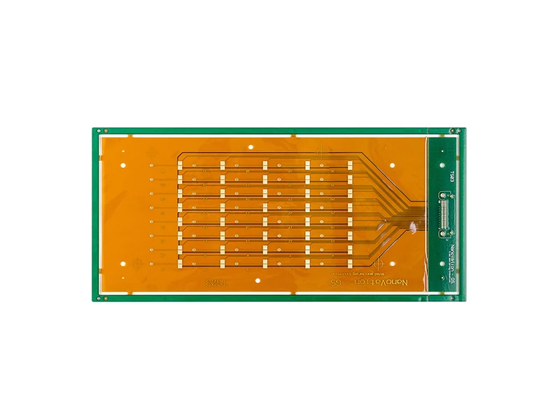
Official catalogue entry 145 · electronic-microscope rigid-flex.
Four-layer microscope board
The published construction is 1R + 2F + 1R, with 1 oz inner and outer copper, 4 mil trace/space and ENIG. The manufacturer identifies dimensional change across the large central flexible area as the difficulty. Its thickness field reads “1.6” without a unit, so confirm the complete rigid and flexible zone thicknesses.
Release datum points, flex-window boundaries, coverlay openings and the installed bend geometry together. Agree the dimensional inspection in both the flat fabrication state and the assembled state. The listed 0.25 mm minimum hole is not explicitly defined as finished-hole diameter.
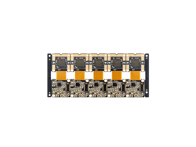
Official catalogue entry 140 · six-layer camera module.
Six-layer automotive camera module
This entry specifies 2R + 2F + 2R, 1.0 mm board thickness, 1 oz inner/outer copper, 3 mil trace/space and ENIG. It calls impedance matching a manufacturing difficulty but supplies no numerical impedance target or tolerance for this board.
Name each controlled net and its reference layer, then request a stack calculation and test coupon for the quoted construction. Include the camera connector, bend and assembly-clearance requirements. The general process table's ±10% is not inserted into this example as a measured result.
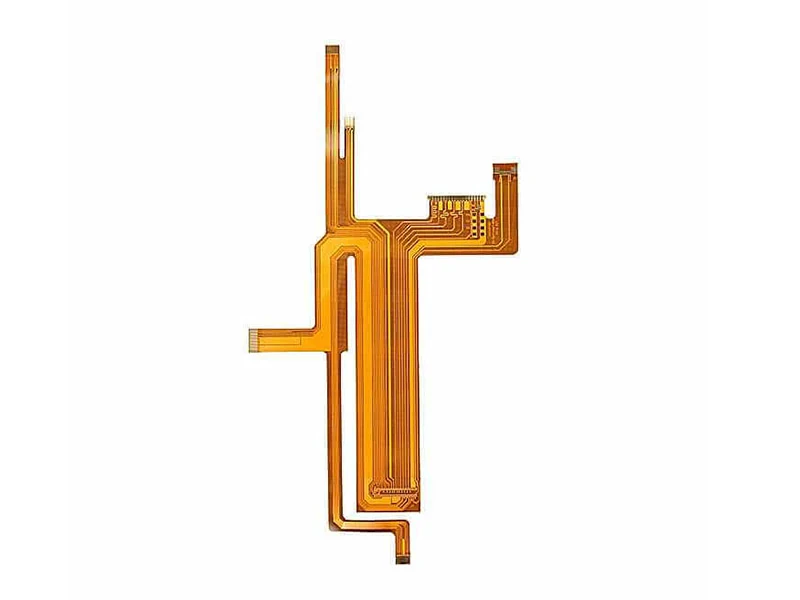
Official entry 112 · original industrial-control FPC image.
Six-layer FPC: 67.8 × 214.6 mm
The example reports FCCL + PP, 0.33 mm thickness, H/H oz copper, 3 mil trace/space and ENIG. It identifies multilayer dimensional change as the process challenge. “FCCL” is a material category, not a purchase-ready laminate grade; the H/H copper notation is retained without assigning weights to unlisted layers.
Define flex zones, bend radius, number of bending cycles and stiffener/connector interfaces. Agree whether the board bends only during assembly or repeatedly in service. The source gives no bend-life test result. Its 0.2 mm minimum-hole field remains separate from a finished-hole acceptance requirement.
Three dated 2024 model notes describe F6G336186A0S sensor control, FCG609001B0S industrial-camera and F4G336187A0S wearable constructions. Their original image and stack-drawing URLs currently return 404, so they are not relabelled with these catalogue photographs. Their manufacturing discussion nevertheless highlights useful release issues: selective plating, NF-PP resin fill, depth-controlled opening and impedance across rigid/flexible regions. Request the actual model drawing before making a model-specific comparison.
DENSITY / TWO DISTINCT PROCESS ROUTES
An eight-layer HDI board and a thick ATE board are different engineering reviews.
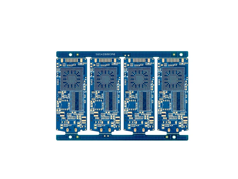
Official HDI entry 114 · video adapter.
Eight-layer, two-step HDI
Stack description
2 + N + 2
Material requirement
TG170; laminate grade unspecified
Board size / thickness
149.2 × 100.5 mm / 1.2 mm
Trace / space
3 / 3 mil
Holes as published
0.15 mm minimum; 0.10 mm laser hole
Finish
ENIG
Release the via spans and each sequential-lamination stage. Confirm which vias are filled, capped or left open, and request the cross-section criteria. The listed 8:1 aspect ratio is a separate source field; it does not mean every laser via has that ratio.
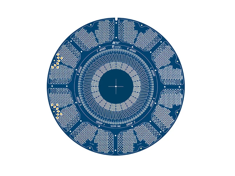
Official special-process entry 117 · IC testing.
26-layer ATE construction
Material / lamination
M6 / M6 + PP
Published size / thickness
380 × 380 mm / 6.6 mm
Copper notation
2 / 2 oz
Trace / space
3 mil
Hole / aspect ratio
0.4 mm / 16:1 as published
Finish notation
“50u” electroplated gold; unit to confirm
The circular catalogue photograph does not define whether the 380 × 380 mm field refers to the delivery panel or the board outline. Request both drawings. The source identifies layer registration as the difficulty; specify registration datums, thickness tolerances, hole-wall acceptance and electrical test coverage before price comparison.
BMS / COPPER BEFORE LINE DENSITY
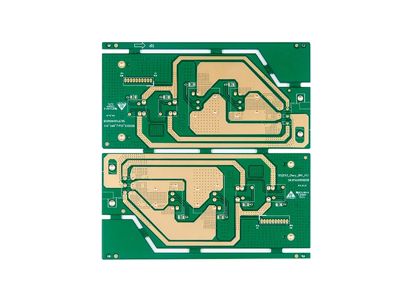
Official double-sided entry 23 · automotive BMS.
Two layers with 8 oz outer copper.
The BMS example gives 1.8 mm board thickness, 8 mil trace/space, 0.35 mm minimum-hole notation and ENIG. The manufacturer explicitly says repeated plating is needed for the 8 oz copper. This is a thick-copper example, not evidence of 2.5 mil routing at that copper weight.
Ask whether the copper figure is the starting foil or the finished conductor requirement and specify where thickness is measured. Release conductor spacing, pad geometry, mask clearances and the plated-hole criteria together. Agree cross-sections at representative heavy-copper features and the solderability requirements for assembly.
PROCESS TABLES / KEEP THE QUALIFIERS
Use the general tables to start engineering questions, not to combine every limit.
Rigid PCB
2–32 layers; 0.25–6.0 mm thickness; 2.5 mil trace/space; inner copper ⅓–4 oz and outer copper ⅓–8 oz. Mechanical and laser drill minima are 0.15 and 0.10 mm respectively, not finished-hole guarantees.
Rigid-flex
2–18 layers; maximum 400 × 540 mm; 0.25–3.2 mm thickness; 2.5 mil trace/space; inner/outer copper ⅓–2 oz. Stiffener, coverlay and rigid/flex outline requirements need separate drawings.
FPC
250 × 250 mm standard and 500 × 500 mm maximum size; 2 mil trace/space; inner copper ⅓–1 oz and outer copper ⅓–2 oz. PI thickness choices range from 12.5 to 100 µm; choose a complete FCCL grade and copper type.
Resolve these source differences in the quotation.
The PCB size field is printed “730mm*620m”; the second unit is malformed. It is not silently corrected into a confirmed panel limit.
The general rigid thickness limit is 6.0 mm, while entry 117 states 6.6 mm. Ask for the special-process route and acceptance for that ATE construction.
The FPC table prints finished thickness ≤0.036 mm while the six-layer example states 0.33 mm. Confirm the complete stack; neither value is substituted into the other.
The homepage says FPC 1–8 layers, but the company introduction says 1–6. The six-layer instance is documented; an eight-layer order needs its own review.
2.5 mil is also printed as 60 µm in the source. Exact conversion is 63.5 µm. Release drawings in one agreed unit rather than treating rounded values as equivalent acceptance limits.
SUPPLIER RELEASE / DOCUMENTS, EQ & DELIVERY
Tie the approval and delivery clock to the actual board and factory.
Qualification scope
The posted SGS ISO 9001 and ISO 14001 copies identify the Shenzhen company and PCB manufacture, with periods ending 5 January 2027. The IATF copy prints 0494664 / CN15/30241, PCB manufacture excluding product design, for 6 January 2024–5 January 2027. Their named Shenzhen location is not automatically certification of the Jiangxi entity.
The hosted flex UL print identifies E529045 with a 2022 update; the Canadian rigid-board print identifies E310444 with a 2021 update. The website's displayed “2025-12-31” dates are not a live UL file check. Obtain the current listed construction and producing location for a compliance-sensitive order. The CQC copy covers a named RCY FR-4 construction, 0.5–1.6 mm, V-0; it does not certify all six examples on this page.
Delivery and engineering release
The delivery page separates engineering questions (EQ), samples of 0–3 m², batches of 10–50 m² and scheduled large-lot deliveries. It also adds time for heavy copper, HDI, half holes, depth-controlled machining and other special processes. A standard table entry is not the final lead time for a board combining several of these.
Ask when the clock starts, whether engineering approval and material procurement are included, and how special-process additions are combined. Define first-lot and repeat-lot delivery dates separately. The website says orders placed after 16:00 move to the next day; confirm the operating calendar and timezone.
The official general contact is sales@szrcypcb.com.cn, telephone +86 755 2970 7148. Its sector contacts also list market7 and market16 mailboxes. No message or mailbox-control test was performed during this research.
Individually researched 8 October 2026. Catalogue images were matched to their own detail links; blank detail-image fields and missing old model images were not replaced with neighbouring products. Seven posted certificate copies were read, without a live issuer or factory audit.