Define the build first. Then choose the production route.
Sichuan Precision Electronics · 四川普瑞森电子有限公司 presents a PCB manufacturing operation at 323 Mingxing Avenue, Innovation Industrial Park, Suining, Sichuan. The official introduction says it was invested in by Shenzhen Bominxing Electronics, with registration/preparation in 2010 and production starting in 2013.
The most useful source is not the website's headline capacity counter: it is the separate volume and small-lot capability table. That distinction matters when moving an RF, automotive power or fine-line design from evaluation to repeat production.
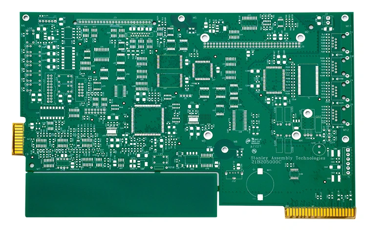
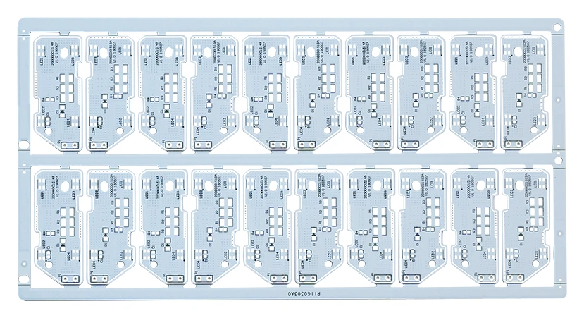
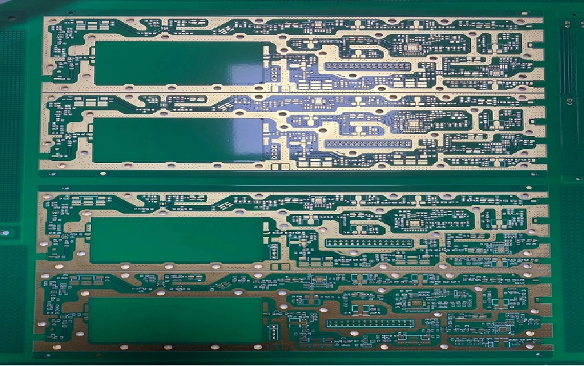
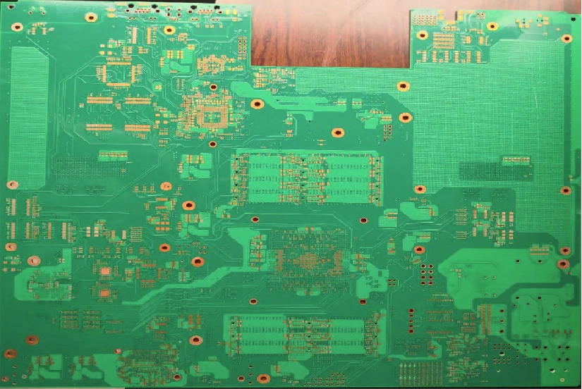
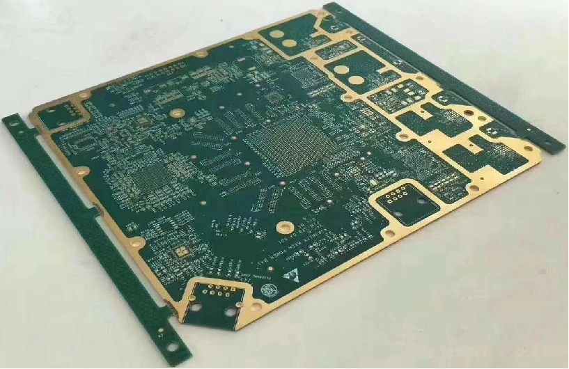
The catalogue below contains fifteen actual board examples. Layer counts appear only where the corresponding product title states them. General line, hole and material ranges stay in their own engineering section; they are not quietly assigned to every pictured board.
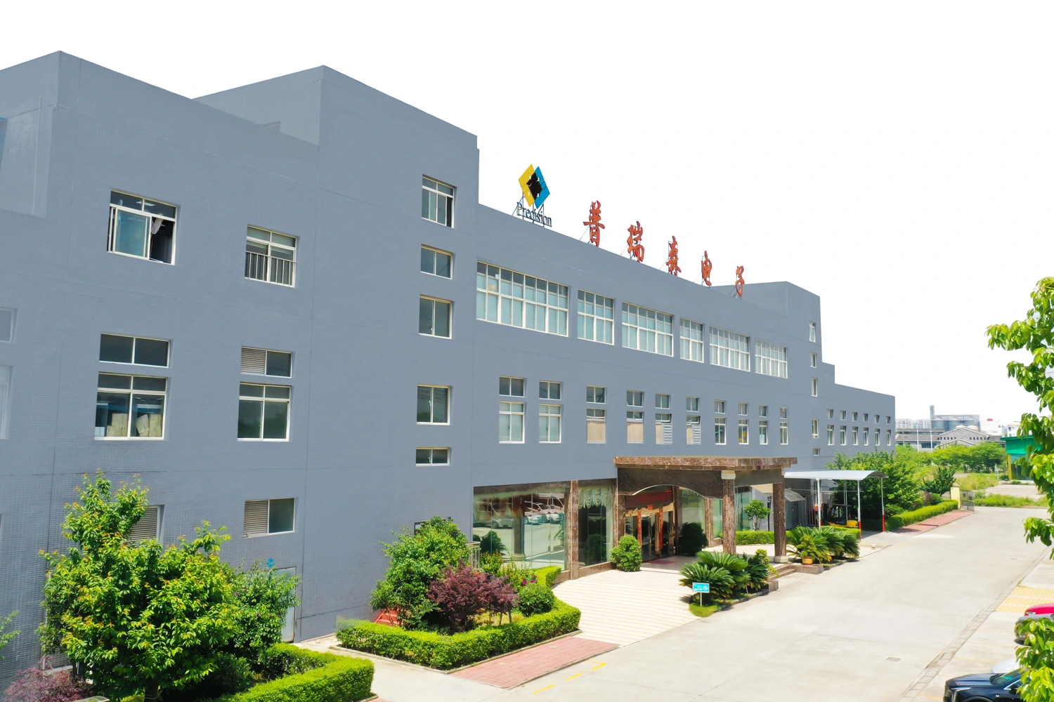
Factory building — original company-page photograph. Site identity and order responsibility still belong in the quotation.
Company dates and capacity figures use different baselines
The introduction says preparation/registration in October 2010 and production in October 2013; the timeline uses September 2010 and November 2013. The homepage also carries a 2001 founding counter. These are not treated as one reconciled legal establishment date.
The timeline's November 2021 lamination expansion states 50,000 m²/month, while the introduction states 60,000 m²/month and the homepage carries 400,000 m²/year. The introduction distinguishes 100 mu site area and 70,000 m² planned construction; those are not the same measure as a workshop-area counter. These undated or historical claims do not reserve capacity today. Ask for the current line/site scope and an available schedule.
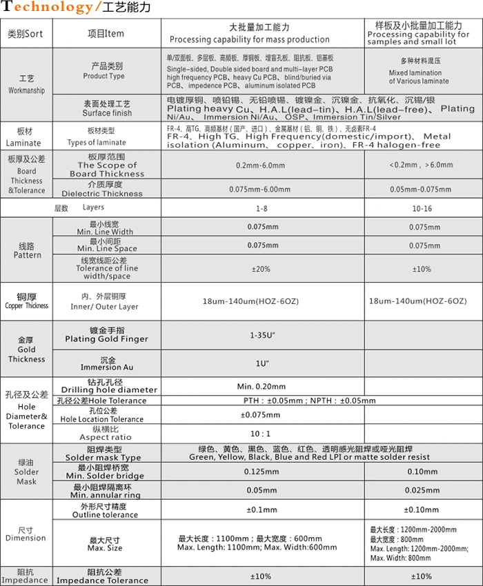
GENERAL RIGID-BOARD TABLE / VOLUME & SMALL-LOT BASIS
A small-lot limit is not the volume-production default.
The official rigid-board chart names single/double-sided and multilayer boards, high-frequency boards, heavy copper, blind/buried vias and impedance-controlled PCBs. Its two columns describe different production conditions. They are useful for an engineering discussion, not proof that every minimum can be combined in your stack.
Mass production
Layers
1–8
Board thickness
0.2–6.0 mm
Dielectric thickness
0.075–6.0 mm
Minimum line / space
0.075 / 0.075 mm
Line/space tolerance
±20%
Solder-mask bridge / annular ring
0.125 / 0.050 mm
Maximum dimensions
1100 × 600 mm
Samples & small lots
Layers
10–16
Board thickness
Below 0.2 mm or above 6.0 mm
Dielectric thickness
0.050–0.075 mm
Minimum line / space
0.075 / 0.075 mm
Line/space tolerance
±10%
Solder-mask bridge / annular ring
0.100 / 0.025 mm
Maximum dimensions
Source length 1200–2000 mm, width 800 mm
Resolve the definitions before quoting
The chart gives a minimum drilling diameter of 0.20 mm, PTH/NPTH hole-tolerance labels of ±0.05 mm, positional tolerance ±0.075 mm and aspect ratio 10:1. It does not define the 0.20 mm figure as a finished plated-hole minimum. Specify finished-hole tolerances and plating separately.
It also lists inner/outer copper 18–140 µm, impedance tolerance ±10%, FR-4/high-Tg/high-frequency/metal-base/halogen-free routes and several finishes. Choose one material, copper, thickness, finish and coupon arrangement. The sample-size length range and missing nine-layer category require order-specific clarification; neither is filled in by interpolation.
For HDI, release the via map, build-up, sequential-lamination plan, material and reliability coupons, and identify processes performed at Suining or externally. The source gives no separate laser-microvia minimum or qualified HDI sequence.
Read the original rigid-board chartOriginal chart. Source rows retain their own definitions and production conditions.
AUTOMOTIVE & POWER / FOUR DIFFERENT ORDER BRIEFS
Separate charging power, equipment control and vehicle lighting.
An on-board charger, charging station, automotive-assembly machine and ambient-light circuit have different functions. Their photographs establish catalogue examples; they do not establish current customer approval, an electrical rating or certification of the completed system.
Original manufacturer catalogue example
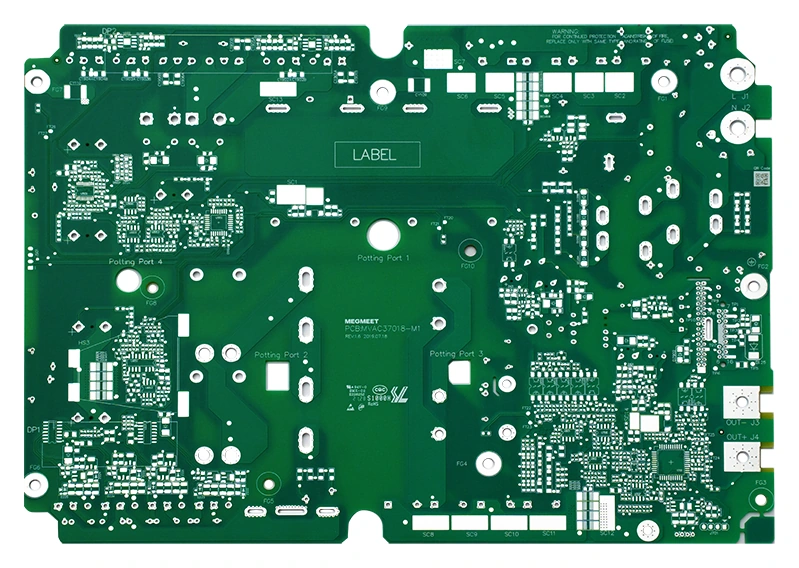
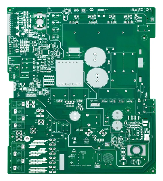
Four-layer on-board charger power PCB
4 layers
Specify power/signal separation, copper weights, creepage and clearance, thermal rise, finished-hole drawings and automotive traceability. The source supplies four layers, not an electrical power rating.
Original manufacturer catalogue example
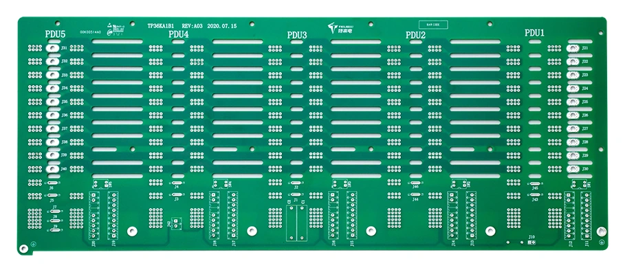
Eight-layer charging-station PCB
8 layers
Confirm finished copper on each layer: the source title writes “30Z” for inner/outer layers, so it is not converted into a guaranteed copper thickness. Include current, temperature rise, isolation and thermal-interface requirements.
This is an equipment-control motherboard example, not proof of approval for a vehicle ECU. Release the eight-layer stack, connector tolerances, interface impedances and functional-system requirements.
Original manufacturer catalogue example
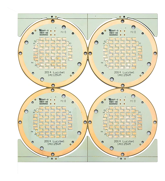
Automotive ambient-light PCB
Not specified for this example
Provide the mounting outline, LED placement, copper and assembly thermal cycle. The title does not identify the layer count or substrate; neither is inferred from its colour.
COMMUNICATIONS, RF & CONTROL / MATERIAL BEFORE MARKETING
For RF, buy a defined laminate and acceptance result.
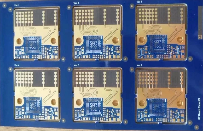
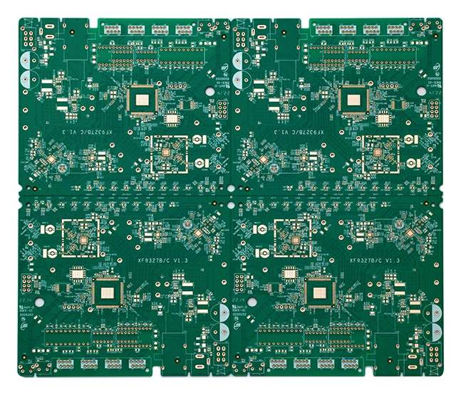
The RF catalogue identifies three different layer structures. None gives a named RF laminate, dielectric loss, measured insertion loss or impedance result for the pictured board. Supply the working frequency and actual stack; a high-frequency title is the starting point for that discussion.
Original manufacturer catalogue example
Six-layer high-frequency communications PCB
6 layers
Name the RF laminate, dielectric data at the operating frequency, transmission-line geometry and impedance coupon. The title gives six layers but no laminate brand, grade or insertion-loss measurement.
Release a laminate grade and a defined Tg test method alongside frequency and loss requirements. High-Tg and halogen-free wording supplies no numerical Tg or substance declaration for your lot.
Original manufacturer catalogue example
Double-sided high-frequency RF PCB
2 layers
Specify the two-sided copper, laminate/bond system, plated-hole process and RF acceptance method. Its gold-coloured pads do not establish finish chemistry or plating thickness.
Interface and control boards
For the router, elevator-control and security examples, release stack, connectors, isolation and mechanical acceptance. Their application titles do not certify the performance or safety of the final equipment.
Original manufacturer catalogue example
Four-layer router PCB
4 layers
Release the four-layer stack, interface impedance targets and connector/assembly panel requirements. Router application wording is not a signal-speed qualification.
Original manufacturer catalogue example
Four-layer elevator-control PCB
4 layers
Define isolation zones, finished holes, outline and netlist testing. An elevator-control board photograph does not establish safety certification of the finished control system.
Original manufacturer catalogue example
Four-layer intelligent-security PCB
4 layers
Provide interface routing, power-rail and mechanical requirements, including the four-layer stack and panel format. The source gives no camera resolution or processing-performance claim.
Five further consumer and lighting catalogue examples
These original pages name applications but do not state layer counts. No layers, surface chemistry or substrate grade are inferred from the photographs.
Original manufacturer catalogue example
LED lighting PCB
Not specified for this example
Confirm whether the design uses FR-4 or a metal base, then define thermal dielectric and mounting requirements. The LED label alone does not make this photo an aluminium-board specification.
Original manufacturer catalogue example
Set-top-box PCB
Not specified for this example
Confirm layer count, connector interfaces, copper and assembly panel. No layer count or finish is published for this individual example.
Original manufacturer catalogue example
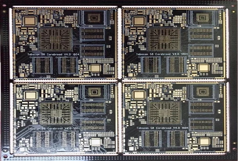
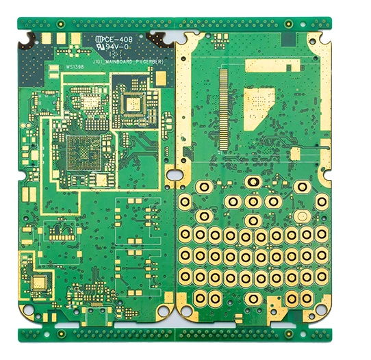
Mobile-phone PCB
Not specified for this example
Send the actual stack and via map. A phone-board application name does not establish an HDI build-up or laser-microvia size for this pictured board.
Original manufacturer catalogue example
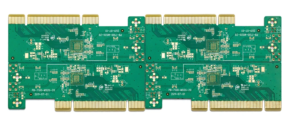
Graphics-card PCB
Not specified for this example
Release edge-contact plating zones, contact thickness, board tolerances and signal-stack requirements. The photograph is not a stated gold thickness, layer count or PCIe qualification.
Original manufacturer catalogue example
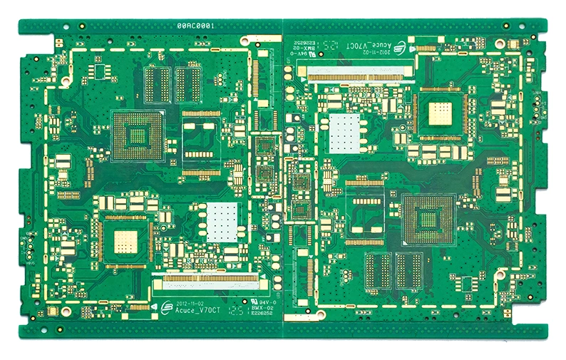
Laptop motherboard PCB
Not specified for this example
Define BGA escape, stack, via construction, impedance and fabrication-test evidence. The source does not identify the layer count or high-density process limits of this example.
METAL-BASE PROCESS TABLE / HEAT AND ISOLATION
Release the dielectric, not just the base metal.
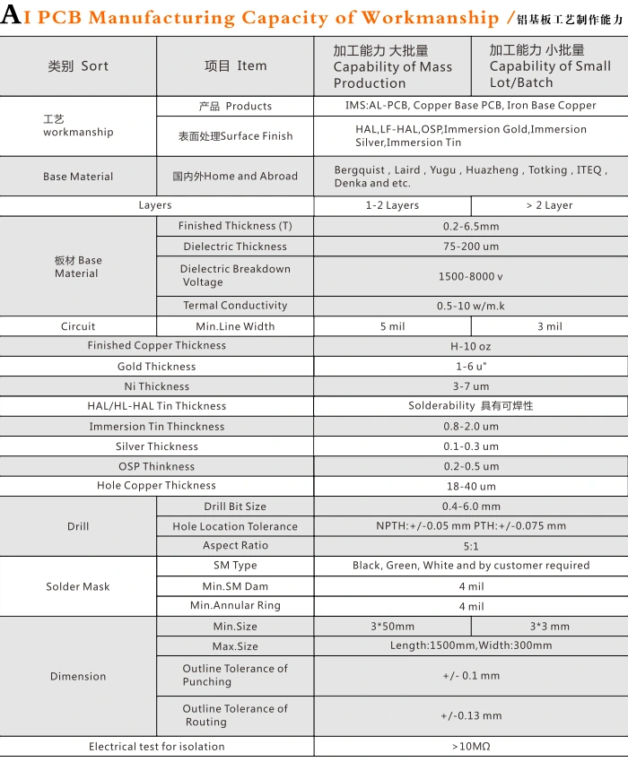
The separate aluminium/metal-base chart lists aluminium-base, copper-base and iron-base circuits. It separates 1–2 layers for volume from more than 2 layers for small lots, and gives 5 mil line width for volume versus 3 mil for small lots. It does not supply a matching minimum line-space pair.
Finished thickness
0.2–6.5 mm, general source range
Dielectric thickness
75–200 µm
Thermal conductivity
0.5–10 W/m·K, no selected material/test condition
Dielectric breakdown voltage
1500–8000 V, no selected construction/test condition
Drill-bit size
0.4–6.0 mm, not a finished-hole minimum
Overall maximum dimensions
1500 × 300 mm, general source limit
The source names Bergquist, Laird, Yugu, Huazheng, Totking, ITEQ and Denka as material references. This is manufacturer disclosure, not a batch purchase or traceability record. Specify the exact material code, base alloy, thickness, copper, thermal interface, isolation conditions and documentation for your order.
The same chart lists H–10 oz finished copper and several finish-thickness rows; the meaning of “H” and the applicability of the broad ranges need confirmation. Do not combine 10 oz, the thinnest dielectric, smallest line and highest voltage into a proved board.
Original metal-base chart, separate from the rigid-board chart and LED photograph.
FABRICATION & TEST / THE MANUFACTURING RELEASE
Convert a capability discussion into a traceable lot.
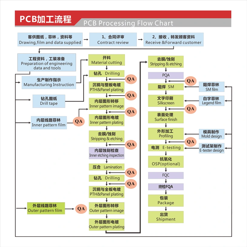
The source process chart starts with contract review and customer data, then engineering/tool preparation. It shows inner-layer processing and inspection, lamination, drilling, PTH/panel plating, outer image and plating, etching, solder mask, legend, finish, profiling, electrical test and final checks. Those are published process steps; responsibilities and any outsourced operations belong in your quotation.
CNC drilling — corresponding source gallery item.
Stack and drilling release
Release the approved stack, laminate grades, copper, via map, tooling and drill/finished-hole definitions. Ask for registration, hole-wall/plating and microsection acceptance appropriate to the actual stack. A general aspect-ratio row does not approve all via geometries.
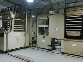
Hot/cold lamination system — source-labelled original.
Lamination and material records
Link the stack to material lots, press cycle and inspection evidence. For high-Tg, RF or mixed materials, ask which laminate/bond combination has been released and what dimensional, dielectric and reliability acceptance applies.
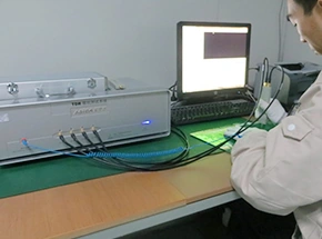
Impedance testing — define coupon and reporting.
Measure the specified transmission line
Define target and tolerance, layer/geometry, coupon, reference method and report format. The presence of a tester and a general ±10% chart row are not an impedance result for the photographed RF examples.
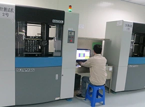
Flying-probe testing — corresponding official gallery original.
Electrical and physical shipment evidence
Agree netlist revision, coverage, isolation/resistance thresholds and report association with the lot. The testing gallery also names AOI, hole checks, nickel/gold thickness, peel, ionic contamination, microsection, withstand-voltage and X-ray checks. Select the tests and sampling required for your design; a list of instruments is not proof that every lot receives every test.
Original process chart and engineering-to-shipment checkpointsUse the actual approved revision and test plan to connect the source process to your order.
QUALIFICATION & RESPONSIBILITY / USE DATED EVIDENCE
Ask for documents with a site, scope and date.
The official Sichuan contact lists 0825-2280000, sales 0825-2511788 and scprsmk@szbmx.com at the Suining address. The mailbox was read from the official site; control was not tested.
Choose the construction. Identify a catalogue example or the general engineering route, then provide Gerber/data, stack, material, copper, holes, finish, quantity and panel requirements.
State the production basis. Confirm volume versus small lot, responsible factory/processes, tooling, engineering approval and repeat-order changes.
Agree shipment acceptance. Release electrical, dimensional, finish, cleanliness, reliability and traceability requirements, with the report formats and lot identification.
Confirm a live schedule. Quote engineering approval, material availability, working-day basis and destination. No undated capacity counter is used as a promised delivery date.
The ISO 14001:2015 copy is 02621E30183R1M, effective 25 May 2021 to 24 May 2024. The SGS ISO 9001:2015 copy CN14/21917 and IATF 16949:2016 copy IATF 0374484 / SGS CN14/20662 show validity from 3 November 2020 to 2 November 2023; the IATF scope is PCB production and excludes product design.
All three displayed validity periods have ended. The webpage calls the IATF image “ISO 9001:2016”; the document itself says IATF 16949:2016. Obtain current issuer details, supplying-site scope and the programme qualification needed for your order. No current certification badge is derived from these copies.
CQC product copy: a limited board scope
CQC 15001125104 is dated 22 October 2020. Its copy lists Sichuan Precision and production code V022136, with BMX-01P / BMX-02P, 0.6–3.0 mm, V-0, under GB 4943.1-2011 and GB 8898-2011. It requires valid surveillance status. This is not a blanket approval of all RF, HDI or metal-base constructions; current register standing was not established here.
2025 monitoring document and historical safety follow-up
The manufacturer publishes a 17-page environmental monitoring report 锡环检字(2025)第0818001号 by 四川锡水金山环保科技有限公司. It identifies the same company/address and sampling on 19–23 August 2025. The report discusses measured emissions/noise under specified conditions; it is neither the operating permit itself nor a statement of continuous current compliance.
For historical context, the government notice dated 4 February 2015 names Sichuan Precision in a major fire-hazard list. The follow-up dated 21 September 2015 explicitly names it among companies that had completed rectification. The adverse record and its follow-up are read together; neither establishes present site safety. Use current documents for supplier qualification.
Substance reports are sample- and date-specific
The download page links older asbestos, PAH, RoHS and a 197-substance REACH report. Those titles alone do not establish today's applicable substance list, your material batch or every surface finish. Request the actual current requirement, material/finish scope and lot-linked evidence; the old link list is not used as a compliance badge.
SOURCE TRAIL
Sources behind this profile
Individually researched 9 October 2026. Fifteen product pages and their corresponding originals, two process tables, four production and two test galleries, factory/history/contact/process pages, four qualification originals and dated original public records. Numerical process rows retain their mass/small-lot bases; unspecified sample parameters remain unknown. Manufacturer-hosted copies and dated public records do not establish current issuer standing, lot approval or reserved capacity.