

Use the standard table for standard boards.
The standard fabrication table lists 1–14 layers, FR-4 or metal-base materials, 0.10/0.10 mm minimum line/space and 0.2–3.2 mm thickness. CNC-routed outline tolerance is ±0.2 mm, compared with ±0.5 mm for V-scoring. PTH and NPTH finished-hole tolerances are listed separately at ±0.08 mm and ±0.05 mm. Copper weight, hole size and special finishes can change cost and review requirements; these limits are not a quotation for every possible combination.
Standard fabrication
Start here for a conventional design that fits the stated stack, routing and hole rules. Specify finished dimensions, copper by layer, surface finish and whether the board is routed or V-scored.
Advanced / rigid-flex review
The separate advanced page includes a roadmap labelled 2016–2018 and a newer-looking, undated process table. Its 64-layer headline is not a current dated production release. The 2/2 mil entries explicitly apply only to portions of the routing and specified base copper. Ask engineering for the current stack and production conditions rather than adopting all maxima.
The dedicated rigid-flex page lists a 26-layer capability, whereas the advanced summary describes a 2–16-layer rigid-flex range. Keep these source scopes separate. For a design outside the photographed examples below, request written feasibility, the production site and its acceptance plan.
Rigid-flex choices start with the installed geometry.
Each photograph below comes from its own official PCBWay product entry. These are examples of manufactured constructions, not stock parts. Parameters stay attached to the corresponding example; hole labels that do not say “finished” are not used as finished-hole filter values.
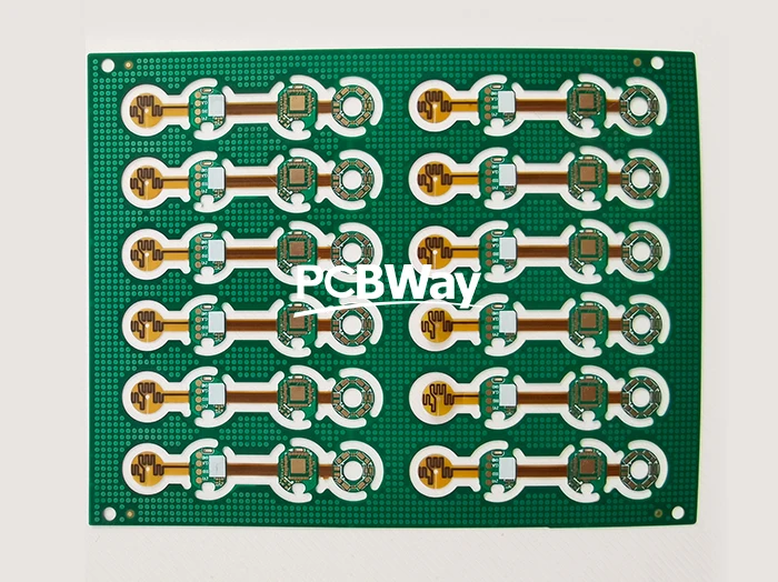
Four layers, 0.35 mm finished thickness.
- Published stack
- 1R + 2F + 1R
- Line / space
- 3 / 3 mil
- Minimum hole label
- 0.20 mm; finished definition not stated
- Material / finish
- Not specified for this example
For a compact enclosure, send the installed bend shape and identify where the 0.35 mm thickness applies. Specify whether the flex is bent once at installation or moves repeatedly, and provide rigid-island and connector dimensions. The photograph cannot establish fatigue life.
The product page calls its use medical electronics; the service gallery calls it industrial control. We retain the construction rather than treating either application label as a qualification.
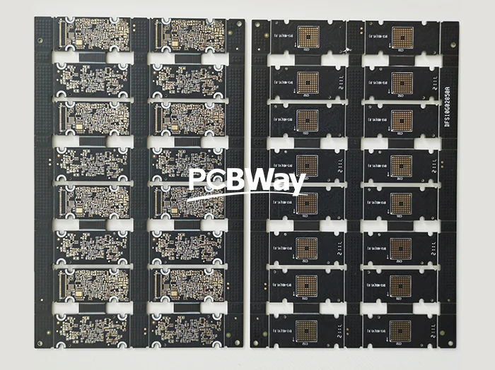
Ten layers with a two-layer flex section.
- Published construction
- 4R + 2F + 4R
- Finished thickness
- 1.0 mm
- Line / space
- 3 / 3 mil
- Minimum hole label
- 1.20 mm; as printed in the official entry
The unusually large 1.20 mm hole label is preserved, not replaced with a smaller general process limit. If the design needs smaller plated holes, ask whether they are supported in the intended stack and what finished tolerance applies.
Define the flex transition, coverlay openings, rigid-zone layer registration and any impedance targets. Agree panel rails, depanelization and assembly handling so that the flex links survive the manufacturing handoff.
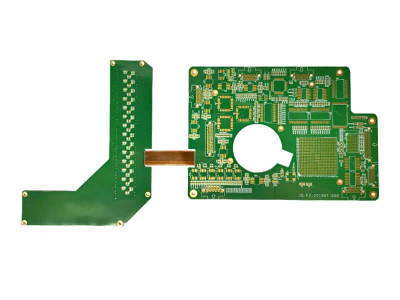
Fourteen layers: DuPont + Shengyi S1000-2M.
- Published thickness
- 2.0 ±0.2 mm
- Line / space
- 100 / 100 μm
- Hole types
- 0.10 mm laser; 0.20 mm mechanical
- Finish
- Immersion gold, described in the product text
The product identifies DuPont material but not its exact grade. Ask for the released laminate and prepreg/adhesive designations, flex copper and coverlay. Attach an approved-substitution rule and request batch traceability for the materials actually used.
Laser and mechanical values belong to different hole types. Specify the build-up, via filling, plating and acceptance separately, along with the drawing revision and thickness measurement locations.
Clarify parts readiness before comparing turnaround.
PCBWay’s assembly table says the turn-time starts when parts, PCB files, BOM, placement data and other necessary documents are complete. It supports consigned, turnkey and mixed sourcing, SMT/THT and single- or double-sided placement. The table gives a five-piece minimum and a 10 × 10 mm minimum board size; smaller or irregular shapes need suitable panelization. The maximum listed size is 250 × 500 mm.
For fine-pitch work it lists 01005 passives, 0.25 mm fine-pitch parts and BGA pitch of 0.3 mm on rigid boards versus 0.4 mm on flex, subject to design confirmation. X-ray, AOI, ICT and functional testing are described, but a list of available methods is not a functional-test specification for every order.
- Procurement releaseControlled BOM, manufacturer part numbers, approved substitutes, consigned quantities, sourcing approval and responsibility for shortages.
- Assembly releaseCentroid data, polarity and reference drawing, panel rails, flex support fixtures, programming files and revision control.
- Acceptance releaseAgreed solder-workmanship class, inspection coverage, X-ray criteria, functional test procedure, rework approval and delivery reports.
The quality page distinguishes standard and advanced test methods and describes Gerber review, microsections, copper-thickness checks, flying probe, AOI and laboratory tests. Request the reports and coverage in the order. Its certificate and IPC-class statements do not establish that a particular board, site or revision has been independently certified by PCBVerified.
Match the brand, the invoice and the assigned factory.
A Shenzhen municipal-government report dated 7 February 2025 identifies PCBWay among the brands of Shenzhen Jieduobang Technology Co., Ltd. (深圳捷多邦科技有限公司), describing production in Longwangmiao Industrial Zone, Fuyong. It establishes a documented brand relationship, not the manufacturing location of every PCBWay order.
The current official About page says its global service works through Hong Kong Yanghui Information Technology Limited. The Hong Kong Companies Registry’s weekly incorporation list records that exact entity as BRN 79076735, incorporated on 4 November 2025. The registry record confirms an entity entry; it does not certify production equipment, beneficial ownership or the factory assigned to an order.
For a controlled production programme, request the contracting entity, actual fabrication/assembly sites and whether processes or sites may change after approval. The service pages describe multiple fabrication and assembly facilities without mapping each catalogue example to a named plant. Support contact information is not a plant assignment.
Official English service contact: service@pcbway.com. Keep board files and requirements tied to the PCBVerified RFQ rather than relying on an undated capability headline.
Compare rigid-flex manufacturers → · Prepare the engineering brief →Sources behind this profile
Individually reviewed on 8 October 2026. Numeric facts stay with their original construction and process scope. The gallery item headed 20 layers but described as 14 layers was excluded. Product photographs retain the manufacturer watermark and full framing. Registry and government records cross-check identity; they do not replace an order-specific plant or process review.
- MANUFACTURER / PROCESS ROUTEStandard PCB capabilities ↗
- MANUFACTURER / DATED ROADMAPAdvanced capabilities and restricted fine routing ↗
- MANUFACTURER / RIGID-FLEXService capability, equipment and gallery ↗
- MANUFACTURER / FOUR-LAYEROriginal product parameters and photograph ↗
- MANUFACTURER / TEN-LAYEROriginal product parameters and photograph ↗
- MANUFACTURER / FOURTEEN-LAYERMaterial, hole types, immersion-gold description and image ↗
- MANUFACTURER / ASSEMBLYParts readiness, geometry and test options ↗
- MANUFACTURER / QUALITYProcess checks and report options ↗
- MANUFACTURER / GLOBAL ENTITYAbout PCBWay ↗
- GOVERNMENT / BRAND RELATIONSHIPShenzhen municipal report, 7 February 2025 ↗
- REGISTRY / ENTITY ENTRYHong Kong weekly incorporation list, entry2578 (PDF) ↗