

A Tongling manufacturer, with a broad control-board portfolio
Tongling Onbole Circuits identifies its company as 铜陵安博电路板有限公司. Its company introduction dates the business to 2014, and its contact page gives No. 999 Xihu First Road, Tongling Economic Development Zone, Anhui. The catalogue's named applications are useful for judging whether your project resembles an existing product family; they do not establish the construction or qualification of a particular order.
For an appliance controller, begin with board dimensions, mounting holes, copper and environmental requirements. For a T-BOX or lighting board, add the applicable customer qualification and acceptance documents. The presence of an automotive example is a reason to ask more targeted questions, not a substitute for the required approval. The Tongling Ecology and Environment Bureau’s 2026 disclosure-enterprise list separately names 铜陵安博电路板有限公司 with unified social credit code 91340700090764417R. That corroborates the named entity in the local regulatory record; it does not certify PCB quality.
The application examples have their own parameters.
These are individually identified boards from Onbole's official catalogue. Their construction tables help explain the company's work more precisely than a factory-wide maximum. The dimensions labelled “minimum hole” are retained as catalogue wording because the images do not define drill versus finished plated aperture.
A six- or eight-layer telematics board
The T-BOX image specifies Mid-Tg material and 0.1/0.1 mm routing. Its description highlights many impedance traces, but gives no tolerance or coupon plan. Those are the two useful follow-up questions for a telematics design.
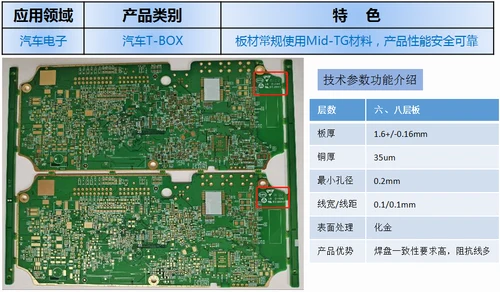
- Published layers
- 6 or 8
- Thickness
- 1.6 ±0.16 mm
- Copper
- 35 μm
- Line / space
- 0.1 / 0.1 mm
- Minimum hole, catalogue label
- 0.2 mm
- Surface finish
- Immersion gold
Ask before quoting: Which laminate grade, stack-up and copper definition support your impedance nets, and what finished holes and test report will be accepted?
A four-layer board with thick outer copper
This charging-controller example specifies 35 μm inner copper and 400 μm outer copper, with a 1.7 mm board thickness. The manufacturer labels it an extra-thick-copper process. Its use of thick outer conductors deserves its own routing and fabrication review.
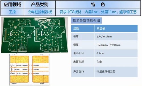
- Published layers
- 4
- Thickness
- 1.7 ±0.17 mm
- Inner / outer copper
- 35 / 400 μm
- Material description
- Mid-Tg requested
- Minimum hole, catalogue label
- 0.5 mm
- Surface finish
- Immersion gold
Ask before quoting: What line/space, copper tolerance, hole-wall and solder-mask rules apply to this thick-copper construction? The 1 oz fine-routing row below is a different condition.
A six-layer controller with fluorescent solder mask
The elevator-controller image lists a six-layer board, 0.1/0.1 mm routing and lead-free HASL. It separately calls out fluorescent green solder mask and yellow legend. The solder-mask and legend requirements therefore belong in the manufacturing brief, not just in an aesthetic image caption.
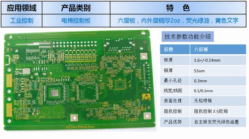
- Published layers
- 6
- Thickness
- 1.6 ±0.14 mm
- Copper, numeric table
- 53 μm
- Line / space
- 0.1 / 0.1 mm
- Minimum hole, catalogue label
- 0.3 mm
- Surface finish
- Lead-free HASL
Resolve the copper wording: The image heading refers to 2 oz inner/outer copper while its numeric table says 53 μm. Ask for starting and finished copper by layer on the current stack-up; neither entry is silently substituted for the other.
3/3 mil has a copper condition.
The three product constructions above sit beside a separate general process reference. The official sheet lists a 1–20-layer range, a maximum finished size of 640 × 540 mm and a maximum thickness of 3.5 mm. Its 3/3 mil line/space value belongs to the 1 oz outer / ½ oz inner copper condition. A thicker conductor, another layer position or a different etch requirement needs its own engineering answer.
| Layer range | 1–20 |
|---|---|
| Line / space condition | 3 / 3 mil at 1 oz outer and ½ oz inner copper |
| Maximum finished size | 640 × 540 mm |
| Maximum thickness | 3.5 mm |
These are separate entries from a process reference. The sheet does not demonstrate that the maximum size, maximum layer count and minimum routing can be delivered together. Its hole terminology also needs clarification before it can be used as a finished plated-hole requirement.
Open the official process-sheet page ↗“±10” changes meaning with the target.
The sheet expresses tolerance relative to the impedance target.
An absolute tolerance. It is not the same as ±10% at a lower target.
As an arithmetic example, ±10 Ω around 50 Ω is a 40–60 Ω interval, equivalent to ±20%. This example explains the unit difference; it is not a measured Onbole result. A buyer needing 50 Ω ±10% should write that requirement explicitly and request a build-specific response.
Define the test, not just the target
Supply the impedance nets, reference layers, proposed laminate and copper. Agree coupon geometry, measurement method and whether the report covers every production panel or another sampling plan. Ask how a target of exactly 100 Ω is treated because the published above/below wording does not resolve that boundary.
Send a copper map with the Gerbers.
- Keep routing and power requirements togetherList starting and finished copper per layer, minimum trace/space, layer count and board dimensions. Ask which entries are compatible in the same stack-up.
- Specify the hole after platingState finished diameter and tolerance, separate non-plated holes, and ask for the corresponding drill allowance. Do not translate a minimum drilling figure into a guaranteed finished hole.
- Write impedance in both formsProvide the target in Ω and allowed deviation in Ω or %. Include the test and report requirement and any restrictions on material substitutions.
Sources behind this profile
Website and process sheet reviewed on 8 October 2026. Process values are manufacturer statements; application examples do not establish order-specific qualification. Catalogue images retain their own product parameters; the factory process sheet is a separate reference. The government list supplies entity context only.
- MANUFACTURER / APPLICATIONSCompany introduction and named catalogue applications ↗
- MANUFACTURER / LOCATIONTongling legal name and contact address ↗
- MANUFACTURER / PROCESSImage-based process capability sheet ↗
- MANUFACTURER / T-BOXSix/eight-layer board image and parameter table ↗
- MANUFACTURER / CHARGINGFour-layer thick-copper controller image and table ↗
- MANUFACTURER / ELEVATORSix-layer controller image and table ↗
- GOVERNMENT / ENTITYTongling 2026 environmental disclosure-enterprise list, entry 121 ↗