

Fourteen layers with third-order HDI build-up.
The dedicated HDI page pairs this red panel photograph with a fourteen-layer, HDI III consumer-electronics example. HDI III describes its sequential build-up; it is a different label from IPC workmanship Class 3. The example has a stated 90 Ω impedance target, but the example table does not supply a tolerance.
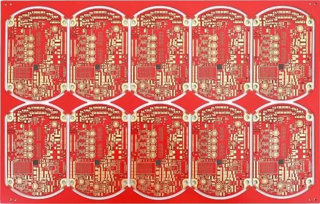
The example names Shengyi Tg170 material, red solder mask and a 0.25 mm minimum BGA pad. It does not identify the laminate grade. Send the approved material designation and full build-up with the RFQ; ask how the blind vias are stacked or staggered, filled and inspected. A blind-via diameter is not a finished through-hole size.
The broader HDI service table lists laser holes of 0.075–0.15 mm, a maximum microvia aspect ratio of 1:1 with 0.75:1 recommended, and filled-via dimple ≤10 μm. These are design-review conditions, not additional measured properties of the pictured panel. Agree the dielectric thickness and microsection acceptance for the actual via structure.
Use the rule for the copper on that layer.
The current standard page lists 1–32 layers. Its routing rules depend on copper weight and whether the conductor is an inner or outer layer. A fine inner-layer value cannot simply be applied to a finished two-ounce outer layer.
| Standard table condition | Minimum trace | Minimum space | RFQ decision |
|---|---|---|---|
| 0.5 oz inner copper | 2.5 mil | 3 mil | Confirm inner base copper and etch allowance. |
| 1 oz outer copper | 3 mil | 3 mil | Specify the finished outer copper requirement. |
| 2 oz outer copper | 5.5 mil | 5.5 mil | Recheck clearances before releasing power routing. |
For standard impedance-controlled boards, the page specifies 4–20-layer default or custom stacks and ±10% tolerance. That statement is narrower than the overall 32-layer range. Supply the impedance targets, reference layers, trace geometry, material and coupon requirement; request the approved stack before committing to fabrication.
The advanced page advertises up to 10 oz copper, while the thick-copper page has a two-ounce maximum row alongside routing entries for 4, 6 and 12 oz. These source scopes do not agree. For heavy-copper work, request a signed copper-by-layer and routing review; this profile does not promote a combined heavy-copper minimum from those conflicting rows.
Choose the flex stack before choosing the connector.
The two photographs are official service-family images. Neither is accompanied by a construction-specific layer stack or measured qualification report. The figures below belong to the corresponding published service tables.
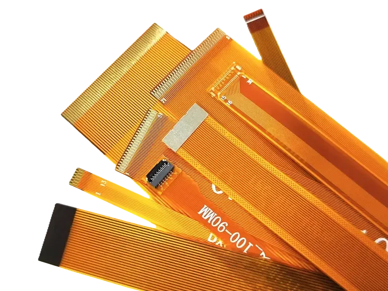
Polyimide flex: copper, coverlay and stiffener.
The flex table lists 1–6 layers, 0.10–0.45 mm thickness, 1/3–2 oz copper and 2/2 mil line/space. Adhesive and adhesiveless constructions, rolled-annealed or electrodeposited copper, PI coverlay or flexible solder mask, and FR-4, PI or metal stiffeners are choices to specify.
Supply the connector insertion zone, exposed-pad geometry, stiffener thickness and installed bend drawing. State whether the flex is bent during installation or moves in service, with the required radius and cycles; the catalogue image cannot establish fatigue life. The named PI suppliers are material options, not proof of a particular purchased batch.
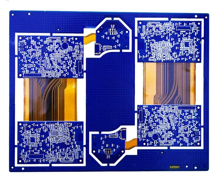
Rigid-flex: one drawing, two process windows.
The rigid-flex table separates the rigid section—2–32 layers, 0.4–3.2 mm, 1–6 oz, 3/3 mil—from the flexible section—1–6 layers, 0.10–0.45 mm, 1/3–1 oz, 2/2 mil. These zone ranges must not be added together to claim a 38-layer construction.
Agree the rigid-to-flex transition, coverlay setback, permitted copper crossings, rigid-zone thickness and flex stack. Specify panel rails and assembly fixtures for the flexible links. ENIG, OSP and immersion silver are listed service finishes; select one for the actual pads and assembly conditions.
The assembly clock depends on parts readiness.
The assembly page describes full turnkey, partial turnkey and kitted sourcing, with HQ Online and global distributors as sourcing channels. Its quoted 24-hour to seven-day turnaround begins after components are ready. Treat parts availability, board fabrication, assembly and shipping as separate dates.
- Approve the boardGerbers, stack, drill definitions, copper per layer, finish, dimensional drawing, test coverage and controlled revisions.
- Approve the partsBOM with manufacturer part numbers, substitutions, consigned quantities, attrition allowance, authenticity requirements and the date all parts will be available.
- Approve the assemblyPlacement/polarity data, flex supports, programming and functional-test instructions, inspection coverage and delivery reports.
The assembly table lists 01005 imperial passives (0402 metric), 0.38 mm fine-pitch ICs and 0.25 mm BGA/LGA pitch. IPC-A-610 Class 2 is the stated default; Class 3 is available on request. SPI, AOI, X-ray, ICT and functional testing are described, but the order must specify which coverage and acceptance criteria apply. A fabrication HDI III label does not select this assembly workmanship class.
Name the production site and the entity on the order.
The manufacturer’s HQ Electronics brochure distinguishes Shenzhen prototype/small-batch PCB production from Jiujiang mass production. It depicts drilling, plating, pressing, imaging and flying-probe operations. The brochure is undated and does not assign the pictured HDI example to a plant; its floor-area and capacity numbers are not treated here as current available production capacity.
Before release, ask which legal entity contracts, which site fabricates, where assembly takes place, and whether a process or site may change after approval. NextPCB’s official support contact is support@nextpcb.com. Keep the technical brief and selected route in the PCBVerified RFQ so that the intended construction remains attached to the request.
Compare HDI manufacturers → · Prepare a complete fabrication brief →Sources behind this profile
Individually read on 8 October 2026. The HDI image is tied to one published example; flex photographs illustrate service families. Mechanical and blind drill values are not finished through-hole minima. Conflicting heavy-copper limits and generic bend-lifetime claims are excluded.
- MANUFACTURER / BACKGROUNDNextPCB About ↗
- MANUFACTURER / STANDARDCopper-conditioned routing, drill definitions and impedance stacks ↗
- MANUFACTURER / HDI EXAMPLEFourteen-layer HDI III panel and microvia conditions ↗
- MANUFACTURER / FLEXPolyimide, copper and stiffener options ↗
- MANUFACTURER / RIGID-FLEXSeparate rigid and flexible zone specifications ↗
- MANUFACTURER / ADVANCEDAdvanced route headline limits ↗
- MANUFACTURER / CONFLICTING COPPER ROWSThick-copper service specifications ↗
- MANUFACTURER / ASSEMBLYParts readiness, placement and test options ↗
- MANUFACTURER / SITE BROCHUREHQ Electronics catalogue (PDF), factory spread pp. 9–10 ↗
- UL / PRIMARY LISTINGE469747 holder and HQPCB-1 board record ↗
- MANUFACTURER-HOSTED / CERTIFICATE COPYNQA IATF certificate for Jiujiang Huaqiu Circuit ↗
- MANUFACTURER / CONTACT ENTITYContact details and return-address restriction ↗
- UK REGISTRY / COMPANY ENTRYEASYFLOW LOGISTICS LIMITED, 16065800 ↗