Start with the interface, then choose the construction.
Mutualtek's catalogue is particularly useful when a circuit must fit a small optical, wearable or packaging interface. Its camera examples combine rigid and flexible regions, air gaps and reinforcement. Its AR entry specifies HDI and EMI features. VCM examples address a flexible connection with steel and polyimide stiffeners; thin substrate examples instead focus on fine routing and assembly surfaces.
The manufacturer identifies the Changshu company as founded in 2006 and publishes a contact at 9 Jinmen Road, Changshu High-tech Industrial Park, Jiangsu. The Chinese entity is 常熟东南相互电子有限公司. The site's wider Mutual-Tek group heading is not a substitute for the entity and production site on a purchase order.
Camera and AR interconnects have different release conditions.
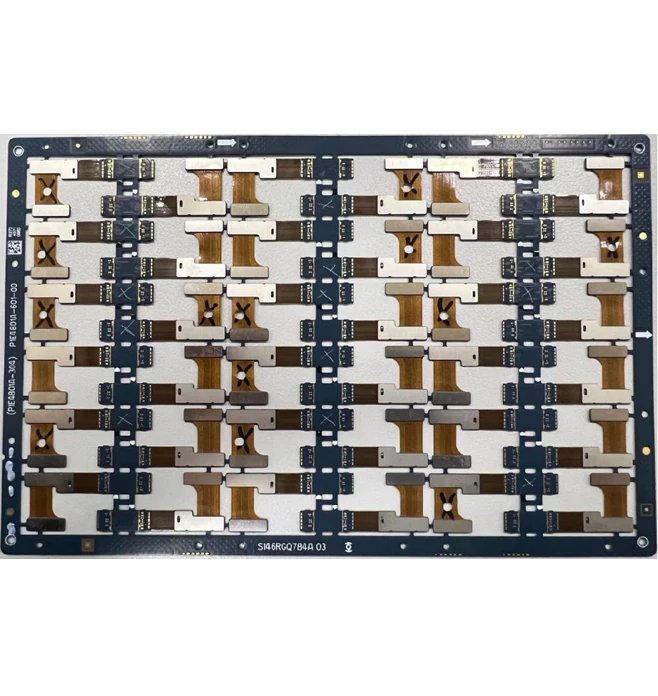
Camera catalogue: S146RGQ784A.
Camera module: air gap and reinforcement
The published structure is 6-4-6-2-6L HDI, BVH, Air-gap. This describes a regional construction; adding those numbers would create an unsupported total layer count. The table specifies NEXFLEX 1810, 0.54 ±0.05 mm thickness, 60/60 µm trace/space and ENEPIG.
Buried diameter / land
0.1 / 0.3 mm
Laser diameter / land
0.1 / 0.25 mm
Reinforcement
C7701 and C7035, each 0.1 mm
Mask / electrical target
PSR-4000 EFB30-S blue; 50 Ω ±10%
Release a region drawing that identifies the air gap, layer transitions, coverlay and metal reinforcement. Ask how that drawing controls installed thickness and planarity at the camera interface. For the 50 Ω target, identify the controlled net, layer, reference plane and coupon; it is a stated example requirement, not a tolerance for every future stack.
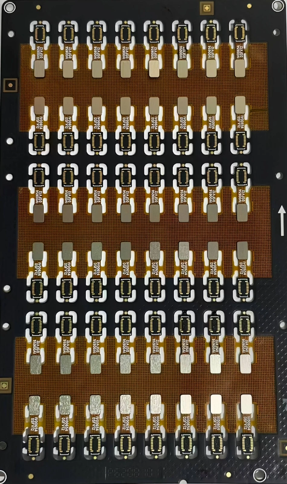
Current AR illustration. Confirm the image and table revision together.
AR eyewear: asymmetric routing and an EMI requirement
The AR table names A118RGQ445A, an 8L HDI+3, Stack Via, EMI construction using DSflex-600. It lists 0.39 ±0.05 mm thickness, 60/40 µm trace/space, 0.35 mm BGA pitch, PI + SUS316L reinforcement and ENIG.
Laser diameter / land
0.075 / 0.25 mm
Buried diameter / land
0.105 / 0.305 mm
Mask
PSR4000 MEH, matt black
Impedance field
N/A in the catalogue table
Do not turn the 40 µm spacing into a 40 µm line-width claim. Define stacked-via locations, filling, the EMI layer and its termination in the actual construction. Establish the BGA footprint and local stiffener flatness with the assembler.
The current photograph carries a different visible board marking from the table's part number. Treat it as an illustration attached to this catalogue entry; obtain the matching drawing and revision before using the table for an order. The photograph cannot resolve that identity difference.
FLEX + STEEL + POLYIMIDE
The OIS interface needs a mechanical drawing as well as Gerbers.
N092FGS469B: two-layer FPC with local reinforcement.
OIS VCM flexible circuit
This example is described as 2L FPC PTH, SUS, Stiffener, using DSflex-600. Its thickness is 0.26 ±0.05 mm, routing is 0.1/0.1 mm and the finish is ENIG. The table names blackened SUS316L at 0.1 mm and PI 6025MT250AL, with PSR-9000 FLX505EM matt-black mask.
The stated PTH diameter/land is 0.15/0.35 mm. The page does not define whether the diameter is a drill or finished-hole measurement; keep the production-stage definition in the drawing instead of treating it as a finished-hole filter.
For an OIS assembly, specify reinforcement datums, adhesive areas, positional tolerance, installed motion and the clearance around moving parts. Request dimensional and functional acceptance for the interconnect supplied. A VCM application label does not mean the PCB manufacturer supplies an assembled or qualified optical stabilisation mechanism.
TWO-LAYER SUBSTRATES / TWO FINISH ROUTES
LED and memory-card substrates are not interchangeable specifications.
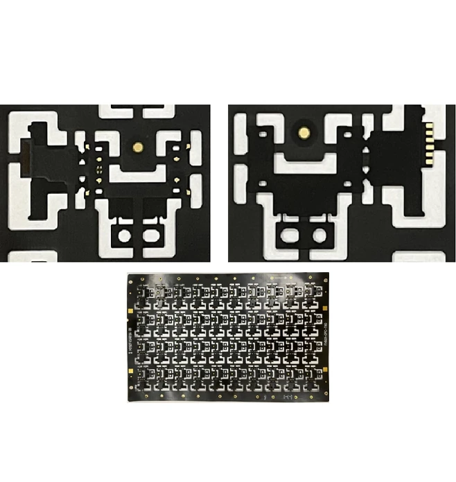
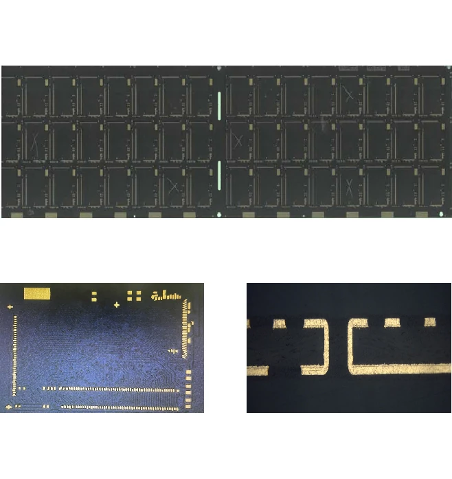
A112PGQ041A / LED catalogue.
LED substrate
2L PTH · SI10U(S) · 0.22 mm · ENIG. This entry gives 37/30 µm trace/space, black solder mask, no cavity and a PTH diameter/land notation of 0.1/0.2 mm.
Release the package land geometry, mask opening, dimensional acceptance and assembly process. The circuit image is not evidence of a populated LED, its optical performance or its thermal qualification in your final product.
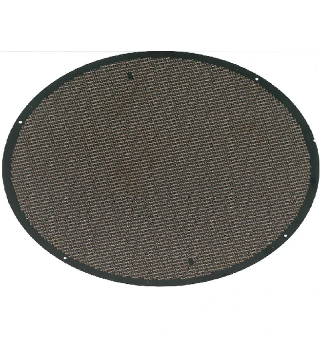
D112PGQ083A / memory-card catalogue.
Memory-card substrate
2L PTH · SI10U(S) · 0.19 ±0.03 mm · ENEPIG. Routing is 75/75 µm. The PTH diameter/land is 0.1/0.25 mm; the entry gives black mask and no cavity.
The W/B pitch field reads 0.076/0.14 mm. Clarify its two quantities against the bond drawing rather than reducing it to a single pitch. Agree the bond-pad finish and assembly acceptance; ENEPIG on this entry is not interchangeable with the LED entry's ENIG.
Both tables name a material, not a supplied batch. Ask for the ordered laminate construction and material traceability linked to the released panel. Neither PTH field defines a finished-hole process stage, and neither entry promises controlled impedance.
ANY-LAYER / TWO ELECTRICAL TARGETS
The server-memory example has its own stack and material.
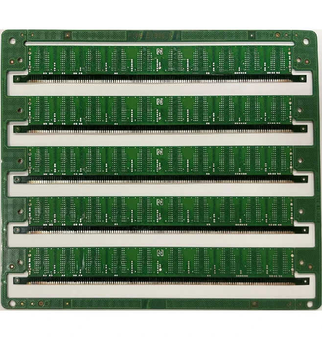
P108RS1986J / server-memory catalogue.
Eight-layer server-memory catalogue board
The entry states 8L Anylayer, Stack Via +3, 2mil PI FCCL, 1.0 ±0.1 mm thickness and 0.1/0.1 mm trace/space. It gives 0.2/0.45 mm laser diameter/land, 0.8 mm BGA pitch, matt-green PSR4000 MPHF and ENIG + ENTEK.
The electrical fields are 100 Ω ±10% and 50 Ω ±10%. Identify the nets, reference planes and test structures for each target. Preserve the named PI FCCL material rather than replacing it with an assumed generic rigid FR-4 stack. The layer count and laser size belong to this example; the generic rigid-board window below describes a different level of information.
BOARD-FAMILY TABLES / DATED OUTLOOK
Choose the process table that matches the released construction.
Rigid-flex table
4–12 layers and 0.21–2.0 mm. Inner-layer routing is 30/35 µm; outer-layer routing is 50/50 µm. The table lists a 0.05 mm minimum hole without defining a finished-hole stage, through-hole aspect ratio ≤8 and blind-hole ratio ≤1.
Its ENEPIG row gives minimum Au 0.05 µm, Pd 0.05 µm and Ni 2.5 µm. Planarity is listed as ≤30 µm before reflow and ≤40 µm after reflow. Agree the measurement region, fixture and reflow conditions before making these acceptance criteria.
Rigid PCB table
2–18 layers, 0.23–2.5 mm and a 600 ×500 mm working panel. Inner and outer routing remain separate at 30/35 and 50/50 µm. Through-hole aspect ratio is ≤12, blind-hole ratio ≤1; the table's 0.1 mm minimum hole is not explicitly a finished hole.
Thickness tolerance depends on thickness: ≤0.5 mm gives ±0.05 mm; above 0.5 and below 1.0 mm gives ±0.08 mm; ≥1.0 mm gives ±10%. Select the applicable row rather than a single tolerance for all boards.
Substrate table
It names Doosan 7409HG_B G type and Shengyi SI10U(S), mechanical drill ≥0.1 mm, UV drill ≥0.04 mm, 30/30 µm routing and 0.3 mm minimum BGA pitch. The listed fill routes are PSR, resin and copper.
These are separate process values. Confirm the chosen fill method, pad construction, solder mask and ENIG, ENEPIG or gold finish against the package drawing. They do not replace the specific LED and memory-card tables above.
Read the 2025 / 2026 Standard and Advance outlook separately
The website labels this fourth table a process capability outlook. Its 2026 Standard column lists inner 30/35 µm on 12 µm copper, outer 50/50 µm on 25 µm copper, 75 µm laser vias and ±10% impedance. The 2026 Advance column gives inner 30/30 µm on 9 µm copper, outer 45/45 µm on 20 µm copper, 70 µm laser vias and ±8% impedance.
Those copper conditions matter. A year column and “Advance” label do not prove every listed item is released together for volume manufacture. Request the dated, order-specific process approval and applicable yield/inspection acceptance from the supplier. The outlook is not used to tighten the six catalogue specimens' specifications.
TRACEABLE LOT / NAMED SITE / ACCEPTED DRAWING
Ask for a traceable first article at the Changshu site.
Link inspection to the production record.
Mutualtek's intelligent-production page describes forward traceability from board-edge, PCS or work-order QR codes to operators, materials, machine times, programmes, quantities, cross-sections, chemical analysis and first-piece inspection. Reverse tracing from equipment codes covers maintenance, alarms and previous production lots. This is the manufacturer's description of its system, not a reviewed record from your batch.
Its equipment pages show laser drilling, UVDI exposure, fill lines, AOI and flying-probe testing. The inspection list includes impedance measurement, planarity measurement, thermal shock, microscopy and mechanical tests. Specify which checks apply to the ordered stack and obtain reports linked to the actual panel or lot; the existence of a machine does not mean every order receives every test.
Release the catalogue part/revision or your replacement drawing, including each rigid, flexible and stiffened region.
Agree material construction, finish, via process, electrical target and assembly interface as one approved specification.
Request a representative first-article record linked to the material lot, process route and required inspection results.
Record the Changshu legal supplier, production location and change-notification conditions for repeat orders.
Individually researched 8 October 2026. Product specifications remain attached to their own catalogue entries; all originals are displayed in full. Hole diameters without a defined finished stage remain outside finished-hole filters. Manufacturer system descriptions, dated outlooks and certificate copies are distinguished from order acceptance.