

MANUFACTURER DOSSIER
Longteng Electronics
湖北龙腾电子科技股份有限公司 · Hubei
Three constructions, three different release decisions.
湖北龙腾电子科技股份有限公司 presents PCB manufacture from development samples through small, medium and large production runs. Its company and contact pages identify the Hubei headquarters in Xiaochang and a Zhuhai Longchang production base in the Fushan industrial area. The product range covers automotive electronics, communications, consumer devices, instrumentation and specialist boards. For procurement, the useful starting point is the actual construction rather than a single maximum-layer number.
The original catalogue photographs and parameters below belong to their named pages. They are manufacturer-published examples, not a test report for a buyer’s design. Each has a different acceptance problem: interconnection reliability, RF geometry or thermal insulation.
An eight-layer board with a defined fine-line rule.
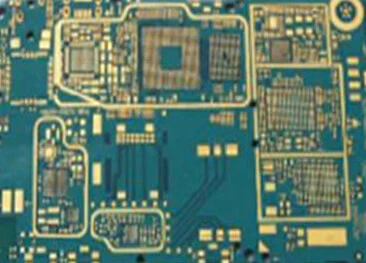
The specific HDI page describes an industrial-robot board with eight layers, buried/blind vias, 3/3 mil line/space, ten IC groups and twelve BGA groups. Its finished board thickness is 2.0 ±0.1 mm, outer copper is listed as 35 µm and the surface finish as electroless nickel / immersion gold.
- Layers
- 8
- Line / space
- 3 / 3 mil
- Finished thickness
- 2.0 ±0.1 mm
- Outer copper
- 35 µm · source definition
- IC solder-mask bridge entry
- 4 / 4 mil
For a robot controller, release the via map and the BGA escape region together. “Buried/blind” does not identify the sequential-lamination count, stacked versus staggered geometry, fill/cap construction or target dielectric. Ask for the proposed stack, copper definition before and after plating, and the land-to-hole requirements on this design. The page does not publish a finished-hole diameter or material grade for the pictured example.
Put these records into the qualification package
Provide the pad and mask apertures, netlist, impedance targets where applicable and environmental duty. Agree which microsections, interconnect reliability checks and electrical results accompany qualification and production. The catalogue’s ENIG description is a finish choice; its nickel and gold thickness, acceptance method and lot record still belong in the order.
Release the laminate pair, not just “high frequency”.
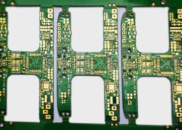
This catalogue entry describes a multilayer construction combining a high-frequency substrate and FR-4. Its technical block identifies “Tu M series” high-frequency material, finished thickness 1.6 ±0.1 mm, copper foil 70 µm, a thick-gold process of 15 microinches and an outline-precision entry of 0.05 mm.
- Finished thickness
- 1.6 ±0.1 mm
- Copper foil
- 70 µm
- Published gold entry
- 15 µin · process to confirm
- Outline precision entry
- 0.05 mm
- Material label
- Tu M series · exact grade required
“Tu M series” is not a released laminate grade or supplier lot. Ask for both the RF laminate and FR-4 grade, bonding sheet, dielectric thicknesses and approved substitutions. The page’s longer background discusses Rogers and historical microwave materials; that background is not evidence that the pictured board uses a particular Rogers grade.
Define frequency range, transmission-line geometry, reference planes, copper roughness requirements and the method used to confirm dielectric properties. The source does not attach an insertion-loss or impedance test report to this board. Also resolve whether the 0.05 mm entry is a bilateral tolerance, a machining accuracy or a particular feature limit: it is not explicitly written as ±0.05 mm.
For the gold finish, name the selective areas, underplate, thickness measurement and solder/contact function. A microinch thickness alone cannot tell the buyer whether the intended interface is soldered, bonded or repeatedly mated. Retain the approved material stack and finish drawing alongside the RFQ.
A copper base changes the qualification question.
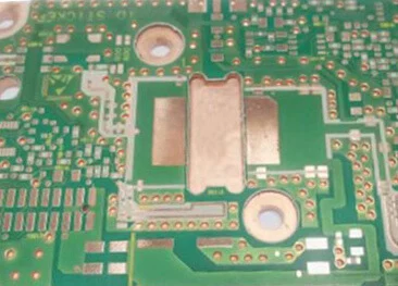
The specialist page lists a copper-base entry with 1.5 mm board thickness and 35 µm outer copper. It gives a menu of thermal-conductivity values—1.0, 1.2, 1.5, 2.0 and 2.4 W/m·K—and separately describes a double-sided copper-base type with withstand voltage ≥4,000 V and a “TG: 170” entry.
- Copper-base board thickness
- 1.5 mm
- Outer copper
- 35 µm
- Conductivity options
- 1.0–2.4 W/m·K · five listed values
- Double-sided entry
- ≥4,000 V withstand · conditions absent
Keep the two type labels separate. The conductivity options are not a single measured value for the photographed board; the page does not identify the layer or test method to which they apply. Ask for the metal base, dielectric system and thickness, copper schedule and interface to the heatsink. Specify whether heat flows through an insulation layer or through a locally defined direct path.
The ≥4,000 V statement is a withstand entry, not a continuous working-voltage rating. Agree AC/DC, duration, leakage criterion, electrode spacing and applicable test specimen. Confirm the unit and test method behind “TG: 170” rather than assuming a fully specified laminate rating. The copper-base block lists surface treatment as “none”; do not add ENIG from the HDI product to this construction. Define exposed-metal protection and solderable/contact areas separately.
Use the labelled production column for a repeat order.
Longteng’s capability page contains a general table and a separate table explicitly labelled sample and volume production. They do not give identical limits. The following comparison retains the original scopes so a successful prototype does not silently become a different manufacturing promise.
Sample column
- Maximum layers
- 30
- Minimum line / space
- 2.5 / 2.5 mil
- Board thickness
- 0.4–7.0 mm
- HDI build-up
- 3+N+3
- Hole spacing entry
- 0.2 mm
Volume column
- Maximum layers
- 26
- Minimum line / space
- 3 / 3 mil
- Board thickness
- 0.4–6.0 mm
- HDI build-up
- 2+N+2
- Hole spacing entry
- 0.4 mm
Both labelled columns list a 570 × 760 mm maximum processing size, 0.15 mm minimum mechanical-drill entry and 0.10 mm laser-hole entry. Mechanical drilling is not a finished plated-hole dimension. The laser thickness-to-hole ratio row renders as unexplained decimal values rather than a usable ratio; it is excluded from numeric matching pending a corrected engineering rule.
Resolve the chart differences before CAM release
The earlier general table lists 1–20 layers, 0.15–5.0 mm thickness, 580 × 700 mm processing area and 0.0635 mm laser drilling. Those figures are not merged with the later sample/volume table. The impedance row in the later chart includes an unexplained “Q” suffix after ±5% and ±8%; obtain a target-specific tolerance and test definition. Numeric impedance matching is withheld until that notation is clarified.
The chart also names mixed lamination, embedded resistance, copper blocks, conductive paste filling, back-drilling and stepped slots. These are process options, not proof that the largest board, finest routing and most complex HDI build-up can be combined. Ask engineering to return one approved design-rule set tied to quantity, copper and plant, with any sample-to-volume changes marked.
Put the fabrication location on the quotation.
The official contact page gives the Hubei location in Xiaochang’s Chengnan industrial park and the Zhuhai Longchang base on Zhufeng Avenue in the Fushan industrial area, Qianwu, Doumen. A group capability table does not assign every machine or construction to both sites. Request the legal fabrication entity, chosen base and engineering contact for the actual order.
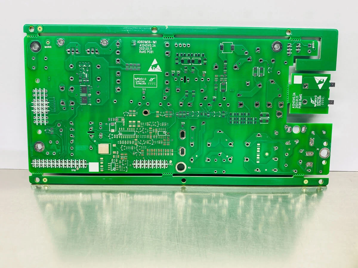
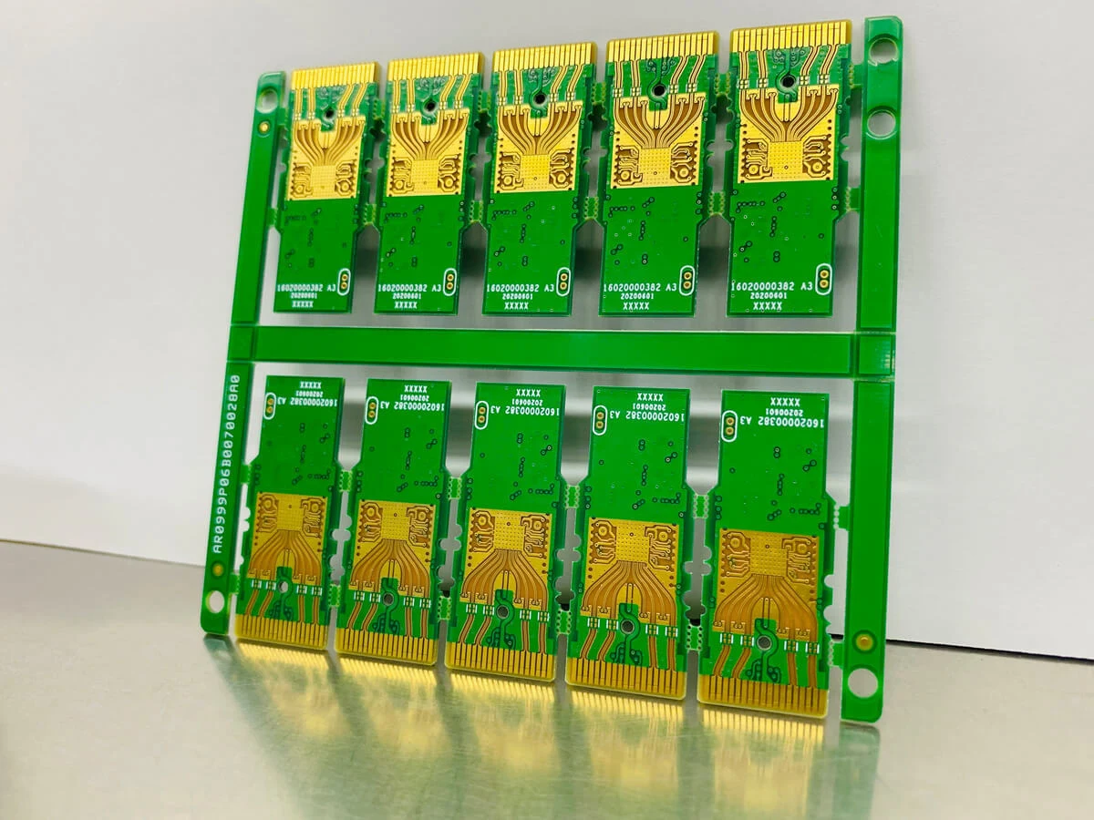
The company introduction discusses ADAS, BMS and charging applications alongside communications, optical modules and industrial controls. For automotive qualification, define the actual customer documentation, traceability and change-control obligations; the introduction’s IATF statement does not establish a current scoped certificate for the assigned plant. For optical modules, release contact geometry, finish zone and stack before comparing the quote with a catalogue photo.
An original Hubei Intellectual Property Office notice published on 13 December 2023 lists 湖北龙腾电子科技股份有限公司 as entry 74 in the new national intellectual-property advantage enterprise list, with a cultivation period November 2023–October 2026. This cross-checks the exact corporate name and that dated IP designation. It is not a factory audit, UL ownership record or a product-quality certificate.
Three items to close before ordering
- Engineering: agreed construction, controlling chart, material grades, finished holes and copper, plus any exceptions.
- Qualification: named plant, applicable certificate holder/scope, coupon and acceptance tests for the selected route.
- Shipment: drawing revision, lot/material trace, netlist results and the agreed RF, thermal or interconnect records.
Sources behind this profile
Reviewed 8 October 2026. Parameters remain attached to individual catalogue entries or their explicit process columns. Manufacturer statements and the dated government identity record have different scopes. Official images are reproduced in their full frame; unknown values and conflicting definitions require order-specific engineering clarification.
- Official companyCompany identity and two production bases ↗
- Official productEight-layer industrial robot HDI ↗
- Official productMixed high-frequency / microwave construction ↗
- Official productCopper-base and double-sided copper-base entries ↗
- Official processGeneral table and labelled sample/production chart ↗
- Official equipmentLabelled production and measurement equipment ↗
- Official contactHubei and Zhuhai base addresses ↗
- Official familyAutomotive catalogue image ↗
- Official familyOptical-module catalogue image ↗
- Government recordHubei IP notice, 13 December 2023, appendix 2 entry 74 ↗