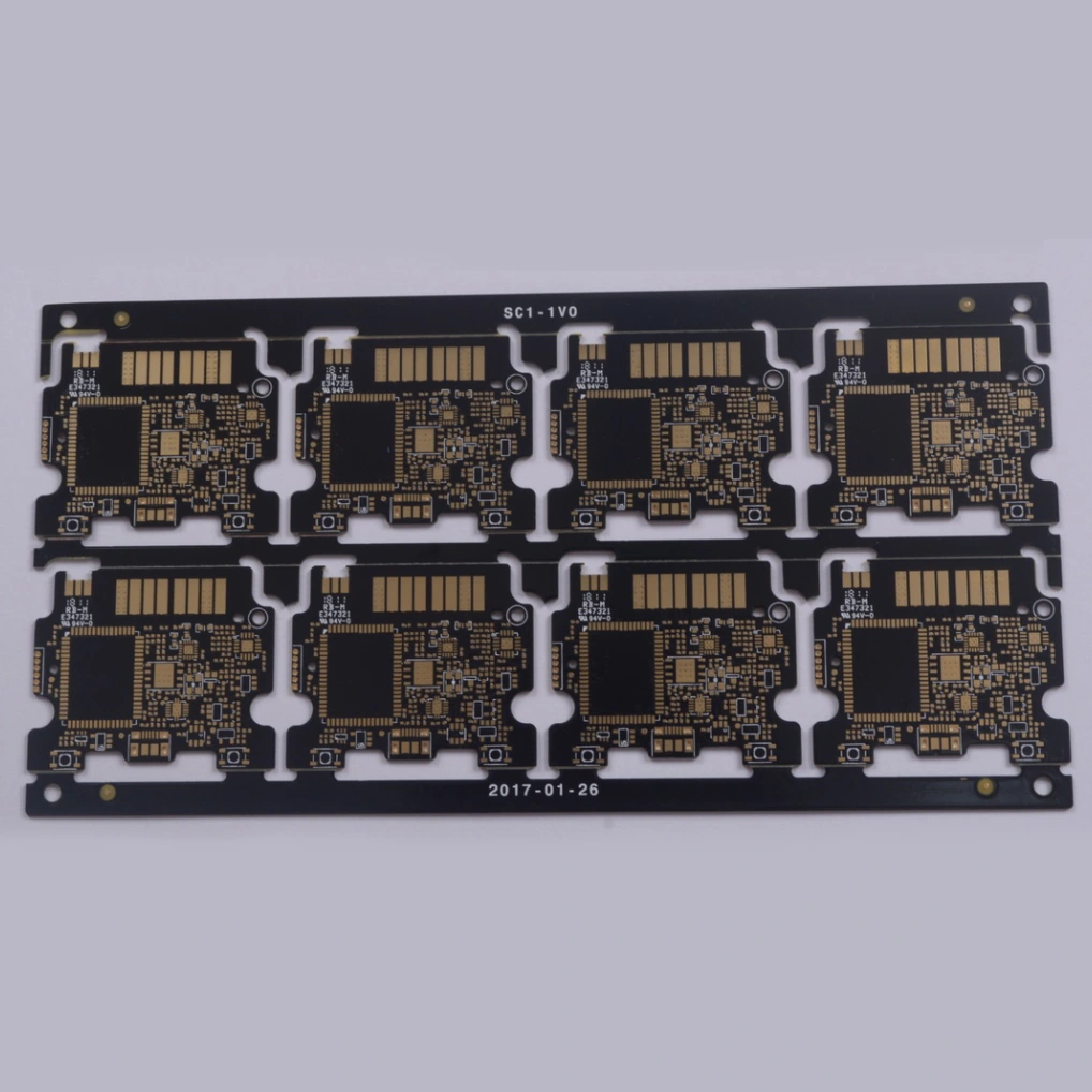
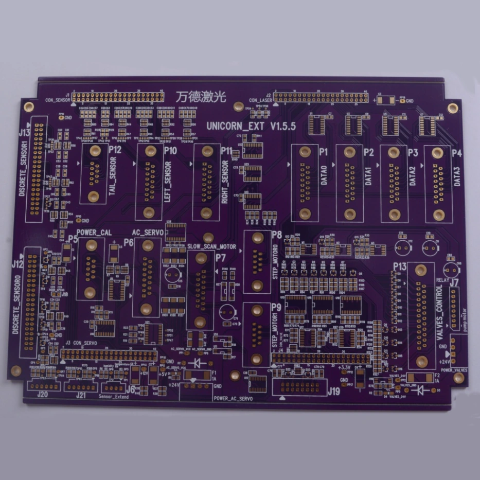
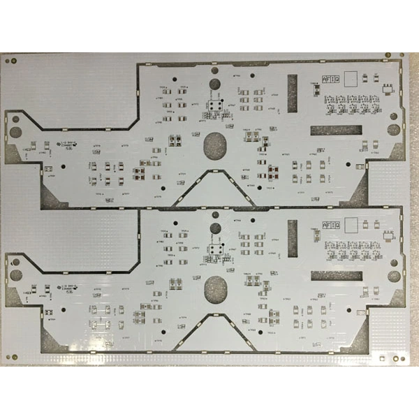
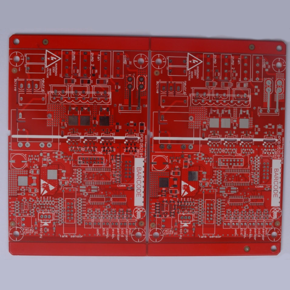
A Huizhou board maker with more than one material route.
Huizhou Liandajin Electronic Co., Ltd. · 惠州市联达金电子有限公司 publishes FR-4 control boards and modules alongside aluminium, ceramic, PTFE and PTFE/FR-4 hybrid examples. Its factory contact and qualification copies locate the business south of Banzhangling, Longshan Sixth Road, Daya Bay West District, Huizhou, Guangdong.
Its introduction traces the business to 2005. The manufacturer-hosted business-licence copy records the Huizhou legal entity's establishment on 4 November 2009, with unified social credit code 914413006981138669. Keep company-history dates and legal registration distinct when specifying the contracting entity.
The practical shortlist starts with your material, actual stack and acceptance plan. A thin eight-layer automotive board, a thick four-layer control board and a PTFE hybrid need different engineering discussions. Twelve catalogue examples below preserve those differences.
FOUR-LAYER FR-4 / INTERFACES & FINISH
Choose the board interface before the finish.
These four examples use FR-4 but differ in thickness, fine-line geometry and surface treatment. The half-hole module needs an edge-plating and solder-joint drawing; the power and industrial boards need copper and thermal or mechanical requirements. Neither is defined by the application name alone.
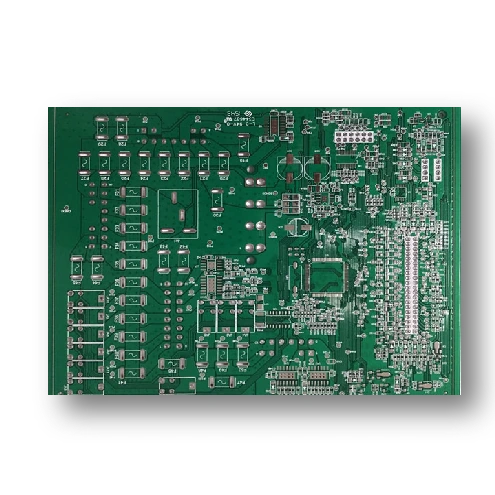
电源控制板 · corresponding original product page
Four-layer power-control PCB
Layers
4
Published material
FR-4
Finished board thickness
1.6 mm
Trace / space
6 / 5 mil (0.1524 / 0.1270 mm)
Published minimum hole
0.2 mm; drill / finished basis unspecified
Finish
OSP
Release the power-net copper, clearance and temperature-rise criteria with the stack and soldering process. This example does not specify copper weight or a voltage rating.
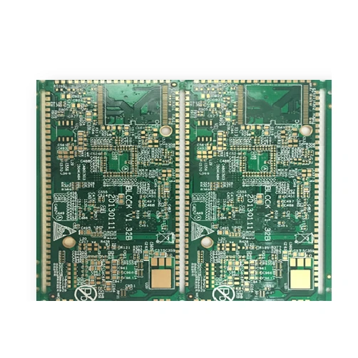
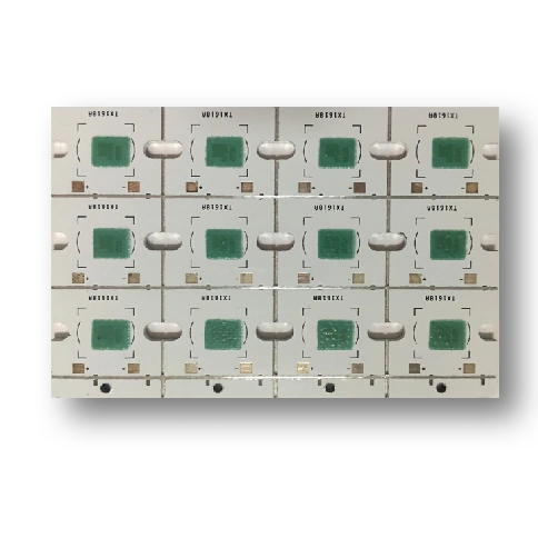
半孔模块板 · corresponding original product page
Four-layer half-hole module PCB
Layers
4
Published material
FR-4
Finished board thickness
1.2 mm
Trace / space
4 / 3 mil (0.1016 / 0.0762 mm)
Published minimum hole
0.15 mm; drill / finished basis unspecified
Finish
Immersion gold
Dimension the castellated edge, plated half-holes, solderable area and routing tolerances; provide the module panel and assembly drawing. The hole value does not define the finished castellated geometry.
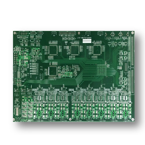
工控板 · corresponding original product page
Four-layer industrial-control PCB
Layers
4
Published material
FR-4
Finished board thickness
2.0 mm
Trace / space
6 / 8 mil (0.1524 / 0.2032 mm)
Published minimum hole
0.3 mm; drill / finished basis unspecified
Finish
Immersion tin
Confirm the 2.0 mm thickness tolerance, connector/mounting interfaces, copper and storage/solderability requirements for the immersion-tin surface.
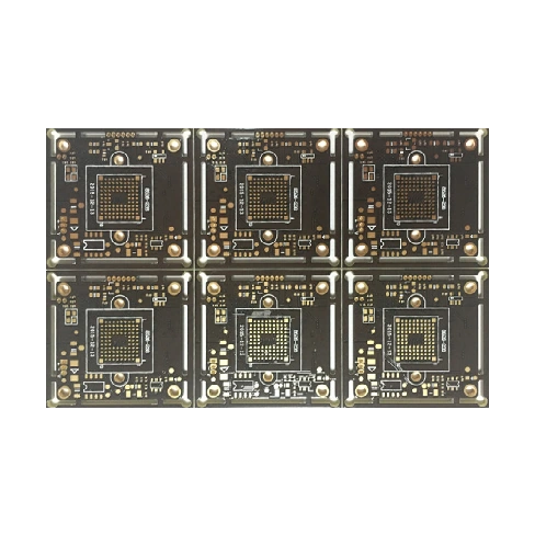
安防板 · corresponding original product page
Four-layer security PCB
Layers
4
Published material
FR-4
Finished board thickness
2.0 mm
Trace / space
4 / 3 mil (0.1016 / 0.0762 mm)
Published minimum hole
0.2 mm; drill / finished basis unspecified
Finish
Immersion gold
Request the actual stack and fine-line process review for this 2.0 mm construction; specify test coverage and pad-finish acceptance. Security is its catalogue application, not a security-product approval.
Translate the drawings, not just the units.
The original pages express line/space in mil; the directory also shows the direct conversion, using 1 mil = 0.0254 mm. Their “minimum hole” fields do not state drill versus finished plated diameter. Those literal values remain visible, but are not treated as confirmed finished-hole filter limits.
Specify the finished hole and tolerance, plating allowance, castellated-edge drawing and inspection locations. OSP, immersion tin and immersion gold are separate finish choices; agree chemistry, thickness where relevant, shelf life and assembly acceptance.
MULTILAYER / STACK, TRACEABILITY & PROGRAMME
Layer count is useful only with its thickness and release package.
The communications example has six layers at 1.2 mm; the medical example has ten at 1.6 mm. Two distinct automotive pages publish two layers at 1.6 mm and eight at 1.0 mm. These are individual construction references, not a promise to combine the finest line, maximum copper and highest layer count.
通讯类板副本 · original photograph, separate construction
Six-layer communications PCB
Layers
6
Published material
FR-4
Finished board thickness
1.2 mm
Trace / space
4 / 4 mil (0.1016 / 0.1016 mm)
Published minimum hole
0.25 mm; drill / finished basis unspecified
Finish
Immersion gold
Provide the six-layer stack, signal references and any impedance targets. No RF loss or impedance tolerance is stated for this individual communications example.
医疗板 · original photograph, separate construction
Ten-layer medical PCB
Layers
10
Published material
FR-4
Finished board thickness
1.6 mm
Trace / space
6 / 5 mil (0.1524 / 0.1270 mm)
Published minimum hole
0.2 mm; drill / finished basis unspecified
Finish
Immersion gold
Specify the device programme, lot traceability, cleanliness and inspection/reliability requirements. A medical application name alone does not establish device approval or a tested medical assembly.
汽车板 · original photograph, separate construction
Two-layer automotive PCB
Layers
2
Published material
FR-4
Finished board thickness
1.6 mm
Trace / space
6 / 8 mil (0.1524 / 0.2032 mm)
Published minimum hole
0.4 mm; drill / finished basis unspecified
Finish
HASL; lead-free status not specified
Set the surface-finish chemistry and thermal/cleanliness requirements, then agree automotive documentation and the supplying site. Do not assume this HASL example is lead-free.
汽车板2 · original photograph, separate construction
Eight-layer automotive PCB
Layers
8
Published material
FR-4
Finished board thickness
1.0 mm
Trace / space
6 / 5 mil (0.1524 / 0.1270 mm)
Published minimum hole
0.25 mm; drill / finished basis unspecified
Finish
HASL; lead-free status not specified
Release a stack and warpage/handling limits for the 1.0 mm eight-layer board; confirm finish chemistry and programme-specific documentation. Its layer/thickness values are separate from the two-layer automotive example.
For an automotive or medical programme, connect the construction to a supplying address, material batch, control plan, change-control procedure and agreed reporting. The qualification copies reviewed below have their own entity, scope and dates. An application label does not make a board a qualified device or approve it for your programme.
ALUMINIUM, CERAMIC & PTFE / DEFINE THE MATERIAL
Four material routes need four different data packages.
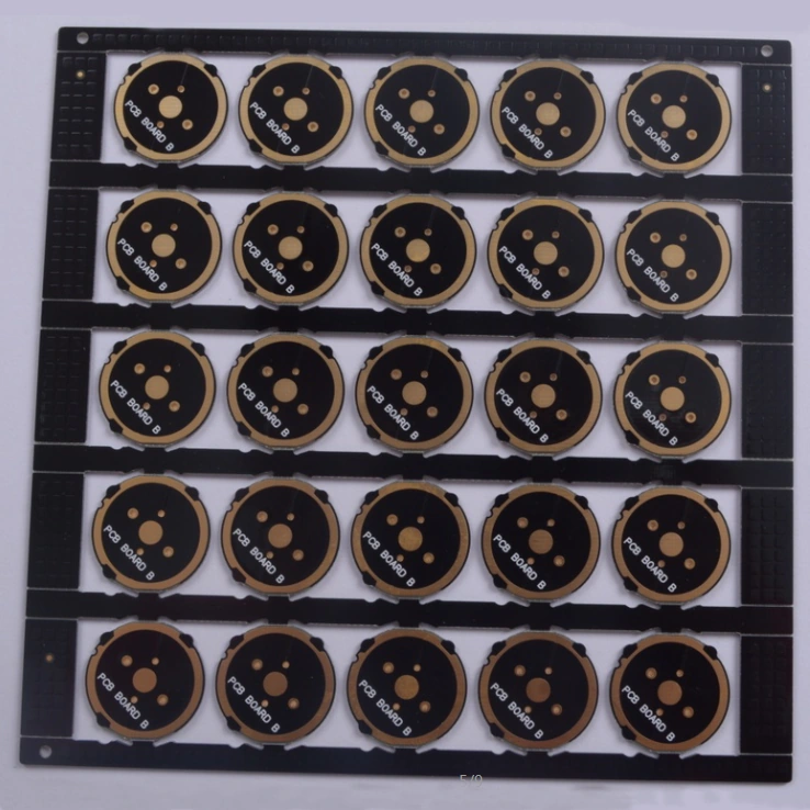
Liandajin's specialty pages supply useful starting geometry, but they do not identify laminate brands, dielectric grades or thermal performance. Use the original example to open a material-specific review, then settle the properties required by your circuit and assembly.
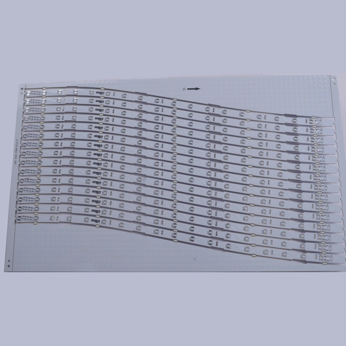
铝基板 · full-size manufacturer photograph
Single-layer aluminium PCB
Layers
1
Published material
Aluminium base; dielectric unspecified
Finished board thickness
1.6 mm
Trace / space
10 / 8 mil (0.2540 / 0.2032 mm)
Published minimum hole
0.4 mm; drill / finished basis unspecified
Finish
HASL; lead-free status not specified
Ask for the aluminium alloy, dielectric thickness, thermal conductivity, isolation voltage and copper. The aluminium label alone does not define a thermal or electrical-insulation rating.
Request the exact ceramic composition, metallisation process, thermal/mechanical limits and dielectric data. Do not infer alumina, AlN, DBC, frequency range or RF performance from the photograph.
铁氟龙 · full-size manufacturer photograph
Single-layer PTFE PCB
Layers
1
Published material
PTFE; grade unspecified
Finished board thickness
2.0 mm
Trace / space
6 / 8 mil (0.1524 / 0.2032 mm)
Published minimum hole
0.3 mm; drill / finished basis unspecified
Finish
Immersion gold
Specify laminate grade, dielectric constant/loss, copper and hole-treatment acceptance at the intended frequency. The page publishes no laminate brand or RF performance.
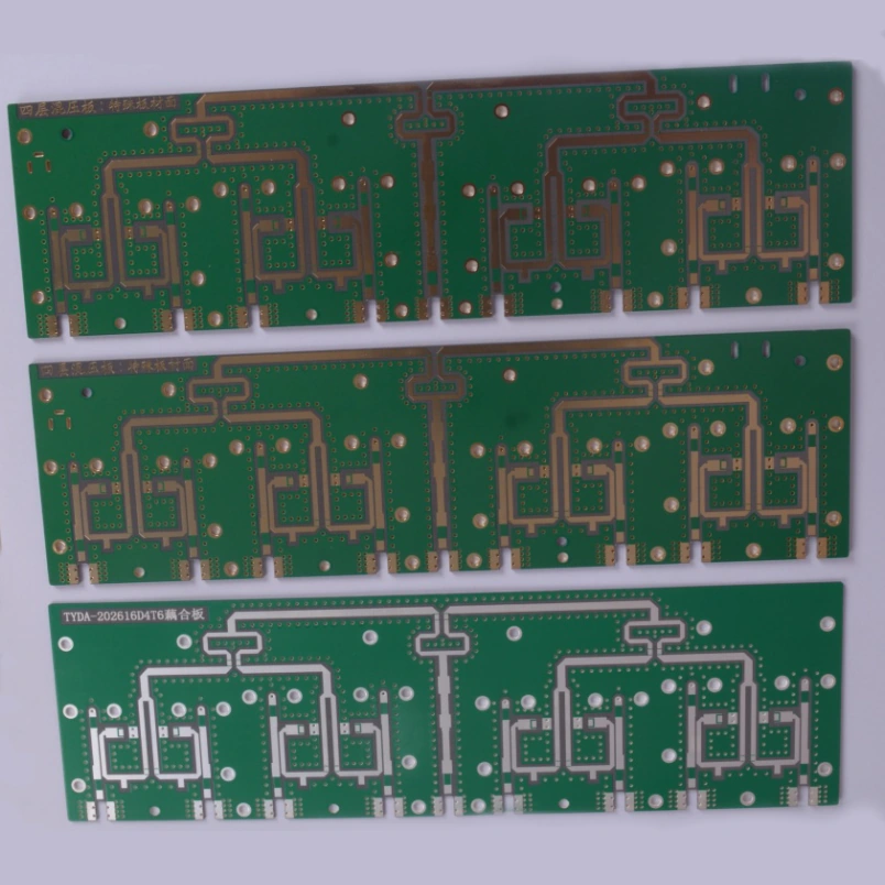
铁氟龙+FR-4混压板 · full-size manufacturer photograph
Four-layer PTFE / FR-4 hybrid PCB
Layers
4
Published material
PTFE and FR-4; grades unspecified
Finished board thickness
2.0 mm
Trace / space
6 / 8 mil (0.1524 / 0.2032 mm)
Published minimum hole
0.8 mm; drill / finished basis unspecified
Finish
Immersion gold is readable; a second finish term is truncated
Provide a layer-by-layer material and bond-ply schedule, pressing cycle, drill/plating acceptance and impedance coupon. Confirm the truncated finish field before quotation; do not assume immersion tin or silver.
The hybrid page has an incomplete finish field.
Its readable Chinese text states immersion gold, followed by an unfinished second term. The second process has not been guessed. Obtain a written finish specification before comparing quotations. The published 0.8 mm minimum-hole figure is also specific to that hybrid example; it is not replaced by the site's general 0.15 mm figure.
For ceramic, request the actual composition and metallisation process. For aluminium, request the insulating dielectric and thermal data. For PTFE and hybrids, release the individual dielectric layers, bonding materials and electrical test coupon. None of these properties can be established from board colour or appearance.
PROTOTYPE TO VOLUME / TWO DIFFERENT CLOCKS
Plan the production handoff as well as the first sample.
The quality page publishes separate sample and volume timing references for two-, four- and six-layer boards. The table below transcribes them; the page does not define working versus calendar days, quantity bands, material readiness, engineering approval or transport.
There is no equivalent published schedule here for the ten-layer medical board or specialty materials. Request a construction- and quantity-specific quotation rather than extrapolating the two-layer sample time.
Before converting the prototype into a repeat order
Freeze the approved revision. Match fabrication files, stack, BOM for materials, drawing and the test netlist.
Release production panels and fixtures. Agree breakaway or V-score, tooling, edge plating and assembly handling.
Confirm the production clock. Quantity, material reservation, engineering sign-off, queue, working-day basis and delivery terms.
Preserve the acceptance package. Approved sample reference, lot records, coupons, certificates of conformity and reports required with each shipment.
The introduction's staff and 60,000 m²/month figures use forecast wording; they are not evidence of available production slots today. Obtain an actual schedule rather than treating the profile as a capacity reservation.
EQUIPMENT & RELEASE / MEASURE WHAT YOU ORDER
Connect the test method to an acceptance result.
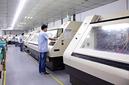
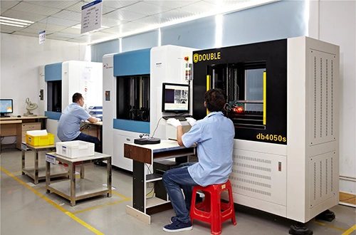
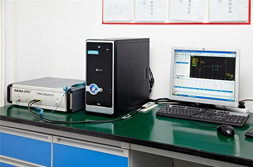
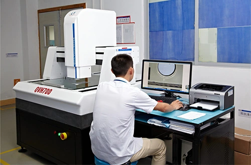
The source-labelled equipment gallery shows drilling, AOI, exposure, etching, electrical testing, impedance testing, coating-thickness measurement, ionic-contamination testing and copper-foil peel testing. The four photographs below are corresponding gallery originals; the gallery does not establish current ownership or utilisation through a site audit.
Drilling machine — official equipment-gallery label.Flying-probe testing — source-labelled photograph.Impedance tester — release the stack, target and coupon.Two-dimensional measurement — define dimensions and sampling.
Electrical and dimensional acceptance
Specify netlist revision, electrical-test coverage and report format, hole and outline tolerances, panel dimensions and inspection sampling. For impedance, agree target, tolerance, coupon geometry, measurement conditions and the report associated with the actual lot; the general ±10% statement is not a test result.
Quality-response expectations
The Q·C·D·S page expresses zero-escape quality goals and a 48-hour countermeasure response. Those are stated policies, not measured defect rates or a guaranteed resolution time. Agree containment, root-cause reporting, replacement and escalation obligations in the order.
For immersion-tin or HASL examples, add solderability, storage and finish chemistry requirements. For fine-line, hybrid or medical constructions, define microsection, cleanliness and reliability evidence appropriate to the use.
ENTITY, QUALIFICATION & ORDER RESPONSIBILITY
Match each document to the supplying site and product scope.
The official contact page publishes ldj@liandajin.com and 0752-5369808 for the Huizhou business. It also lists regional marketing contacts. The Shanghai entry has a separate company name, Shanghai Liandajin Circuit Co., Ltd.; do not treat every sales office as the production site.
The public mailbox was read on the official site; control of the mailbox was not tested. Keep the enquiry on PCBVerified using the construction shortlist, and request the exact quoting entity, factory address and scope of any subcontracted process.
The environmental disclosure includes manufacturer-hosted historical approval, acceptance and monitoring files, including 2022 monitoring records. Their presence is not a current environmental-compliance conclusion.
The Intertek IATF 16949:2016 copy identifies IATF 0516388 / 2012-0464, site code CAFMP6, issued 12 May 2024 and valid until 11 May 2027. Its scope is manufacture of printed circuit boards; product design is excluded.
The ISO 13485:2016 copy is 0078499-02, issued 2 July 2024, valid until 22 July 2027, for production of PCBs for medical devices at the Huizhou address. It is a management-system scope, not approval of a medical device.
These are manufacturer-hosted copies. Current issuer-register standing and the qualification of your specific lot require confirmation.
ISO, GJB and the limited CQC product scope
The ISO 9001, ISO 14001, ISO 45001 and GJB 9001C copies show effectiveness from 5 September 2025 to 11 September 2028. Their respective registration numbers are 02625Q31160R3M, 02625E30226R3M, 02625S30225R3M and 02625J31887R4M. The listed PCB scopes must be matched to the order.
CQC 19134216549 is dated 21 November 2025, valid until 20 November 2030. Its copy specifies LDJ-2 multilayer boards, 0.6–3.2 mm and other stated conditions. It is not a blanket certification of every aluminium, ceramic or PTFE example in this profile.
UL: a historical directory print, not a current ownership badge
The framed directory print identifies E344687 and Huizhou Liandajin Electronics Co. Ltd. It is marked last updated 26 May 2011. That historical copy is retained as such; current UL file-holder status, recognised constructions and material conditions were not established from a live registry in this review.
If UL recognition is required, obtain the current listing and construction details for the supplying entity and compare the actual materials, thickness, temperature and flammability conditions with your design.
SOURCE TRAIL
Sources behind this profile
Individually reviewed 9 October 2026: twelve original product pages and full-size photographs, eighteen equipment images, nine qualification copies, company/contact/quality/technical pages and the live government maintenance list. Hole basis and laminate grades remain unspecified. Lead times are undated source references; certificate-copy dates do not establish current register standing or lot approval.