Different board families need different release drawings.
Kunshan Huaxin's public catalogue reaches from double-sided and multilayer rigid boards to HDI, flexible circuits, rigid-flex and aluminium-base boards. The website is operated under 昆山华新电子集团有限公司; this directory record's Chinese legal name is 昆山市华新电路板有限公司. A 20 November 2025 Kunshan government report identifies that company as a Huaxin group subsidiary. Keep the supplier named on the purchase order distinct from the wider group catalogue.
The company history starts in 1993 and names Huaxin, Huaxing and Jiangsu Huashen within the group. Its board examples are more useful for an engineering conversation than a single maximum-capability number. One photographed HDI specimen has a readable specification card; several other product entries publish only a construction name. The routes below preserve that difference.
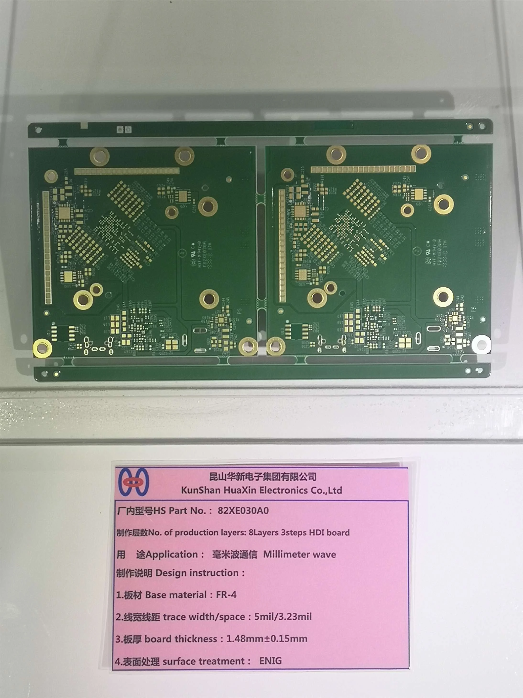
An eight-layer HDI example with a usable specification.
Complete original board and specification-card photograph. Catalogue entry 44.
Eight-layer, three-step communications board
The official product title calls this an eight-layer, three-step communications board. The printed card names part 82XE030A0 and describes a millimetre-wave application. Its published characteristics belong to this catalogue example.
Layers / HDI steps
8 / 3
Base material
FR-4; grade not named
Trace / space
5 / 3.23 mil
Board thickness
1.48 ±0.15 mm
Surface treatment
ENIG
The line and space values differ: approximately 0.127 and 0.0820 mm. They are not a 3.23/3.23 mil capability. The card does not specify the finished hole, via-fill method, dielectric brand, operating frequency, loss measurement or impedance tolerance.
For a communications design, provide the actual frequency range, critical transmission-line geometry and stack. Ask which FR-4 grade and copper construction support the loss and electrical acceptance requirements. An application label alone does not qualify this board for your RF channel.
For the three-step HDI structure, agree the layer interconnection map, microvia construction, filling and inspection records. Define reliability acceptance for the actual stack rather than deriving a via arrangement from the photograph.
SOLDERING INTERFACE / LAYER STACK
Two rigid-board examples answer different questions.
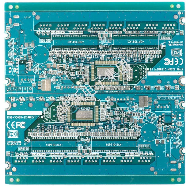
QFP chemical nickel-gold PCB, catalogue entry 56.
QFP board with chemical nickel-gold finish
The manufacturer identifies the package application and finish. Its page does not publish the layer count, pad pitch, nickel/gold thickness or laminate for this specimen. The displayed 0.00 catalogue price is not a quotation.
Release the component footprint and pad dimensions with the solder-mask openings, finished-board flatness and the intended soldering process. Agree finish thickness and acceptance records for the lot. This example is a starting point for a QFP assembly interface, not proof that every fine-pitch footprint is covered by one finish declaration.
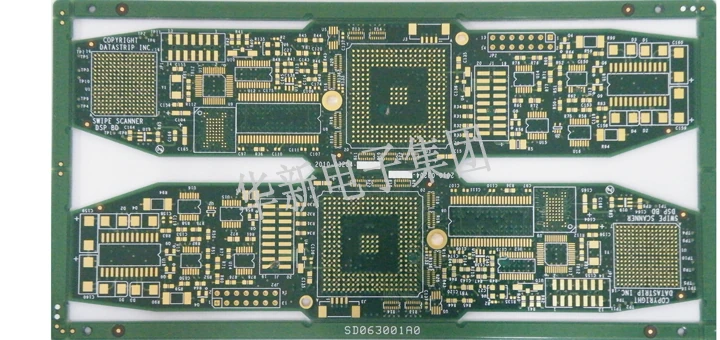
Sixteen-layer board, catalogue entry 60.
Sixteen-layer multilayer board
The product title gives a sixteen-layer construction. It does not give a per-layer copper schedule, finished thickness, hole dimensions or impedance result. The homepage's separate “4–10” multilayer heading does not negate this specific sixteen-layer catalogue entry.
Send the proposed stack and identify the electrical, power and mechanical functions by layer. Establish the laminate and prepreg schedule, finished thickness, drilling requirements, panel arrangement and the electrical test. If the design has press-fit or controlled-impedance features, add their explicit acceptance requirements; neither is established by this image.
FLEXIBLE REGION / TERMINATION / INSTALLED SHAPE
Define where the interconnect bends and where it connects.
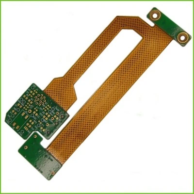
Rigid-flex example, entry 84.
Rigid-flex assembly interface
The product page names rigid-flex but gives a general flexible-circuit explanation rather than the illustrated part's stack. Its 0.1–0.3 mm sentence concerns a general flexible-circuit thickness; it is not an approved overall thickness for this rigid-flex board.
Define rigid and flexible regions separately, including coverlay, transition zones, stiffeners and the final installed shape. State whether the flex is bent once during installation or moves in service. Agree bend radius and test duty from the actual material and copper construction; the site's broad flexibility language does not establish unlimited bending or cycle life.
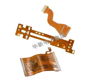
Single-sided flexible circuits, entry 83.
Single-sided flex for a defined termination
This entry explicitly identifies a single-sided flexible board. Its image contains several examples; it does not supply connector pitch, trace width, copper weight, surface finish or stiffener dimensions.
Release the contact drawing and required finished contact thickness, the conductor outline, coverlay openings and local reinforcement. For a soldered, inserted or bonded termination, name that process and the assembly fixture. Do not infer an approved connector fit from the appearance of the pictured fingers.
GROUP CONTACT / MANUFACTURING-SITE RECORD
Resolve the site address before qualification.
Three addresses have different meanings.
The official contact page gives the group contact at 301 Hongyang Road, Qiandeng, Kunshan, with telephone 0512-57476666 and webmaster@kshuaxin.com.cn. That is a published website contact, not a confirmed sales-response or deliverability test.
Suzhou's 10 June 2023 environmental approval, 苏环建〔2023〕83第0259号, names 昆山市华新电路板有限公司 and a proposed relocation to 191 Qipu West Road. It describes moving the original 1618 Qinfeng South Road factory and merging the first manufacturing-zone content of Kunshan Huaxing. The planned output after completion is 1.2 million m² of PCBs annually.
The approval establishes a named project and its conditions. It is not evidence that the relocation is now complete or that the planned output is available for your order. Ask for the current fabrication and shipment address, contracting entity, process allocation and any transition affecting repeat production.
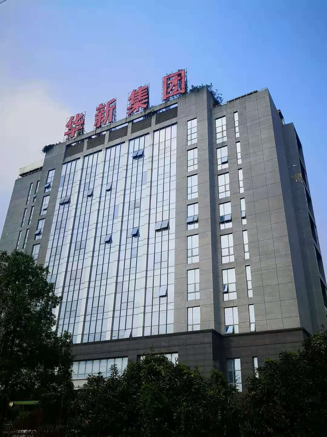
Official group building photograph. No street address or production-line allocation is inferred from it.
Government identity and environmental context
The Kunshan government's 20 November 2025 report identifies Huaxin Circuit Board as a subsidiary and reports its inclusion in the Jiangsu green-factory context. It discusses water reuse and resource recovery. This is relevant to entity and environmental due diligence; it does not establish electrical yield, a customer-approved stack or certification of each product.
Equipment and certification claims
The official introduction and exhibition text describe PCB/FPC production and inspection equipment, including laser drilling, CCD exposure, VCP plating and AOI. These are manufacturer descriptions without a current, site-allocated machine inventory. The website also names UL and management-system certifications, including historical QS9000 and ISO/TS16949 language. Obtain current certificate numbers, scope and site coverage for the proposed plant; no certification badge is awarded from those general statements here.
ONE QUOTATION / ONE APPROVED CONSTRUCTION
Keep these decisions together when requesting a quotation.
Name the manufacturing entity.
Record the legal supplier, fabrication address and any subcontracted process. Keep group correspondence and production qualification linked to the same order.
Choose the relevant catalogue route.
Use the eight-layer specimen card for an HDI discussion, the sixteen-layer entry for a multilayer stack, or the flex examples for mechanical interfaces. Attach the actual drawing and revision; the selected example is not an approved production specification.
Release the materials and acceptance records.
Agree laminate grade, copper, finish, finished holes, dimensions, test method and any RF or bend-duty requirement. Ask for a documented DFM response and first-article evidence against those requirements.
Plan repeat production at the agreed site.
Confirm material lead time, production location and change-notification conditions. The differing group capacity and headcount statements on the website are not used to estimate current lead time or available throughput.
Individually researched 8 October 2026. Catalogue titles, readable specimen labels, group statements and dated government records are kept separate. Original images are displayed in full; unanswered order-specific specifications remain open. Existing factory and legacy product URLs are preserved.