

Three board families, three different release packages.
The photographs belong to Kinwong’s HDI, RF and copper-inlay service pages. They illustrate those families; the website does not give a complete construction specification for each pictured panel. The process values in this profile stay attached to their stated process or application.
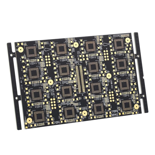
01 / DENSE INTERCONNECT
Choose the routing process before releasing the stack.
The HDI page separates 30 / 30 μm line/space for mSAP from 40 / 40 μm for tenting. It also names any-layer structures and ±1 mil solder-mask alignment. These are process statements, not a single approved construction for the photograph.
Supply the escape geometry, finished copper, dielectric build-up, microvia sequence and reliability requirements. Ask the field application engineer which route and plant can reproduce the design at your order volume.
Website: process-specific routing
mSAP 30/30 μm and tenting 40/40 μm remain separate. The introductory HDI definition of a microvia at or below 0.15 mm is not Kinwong’s finished-hole production minimum.
2025 report: application-specific disclosure
The automotive table gives HDI up to five build-up stages and 60/60 μm routing. The communications/data-infrastructure row gives up to eleven stages, 60 μm blind holes, 150 μm spacing and 30/30 μm routing. These are different application scopes; the hole values are not finished through-hole specifications.
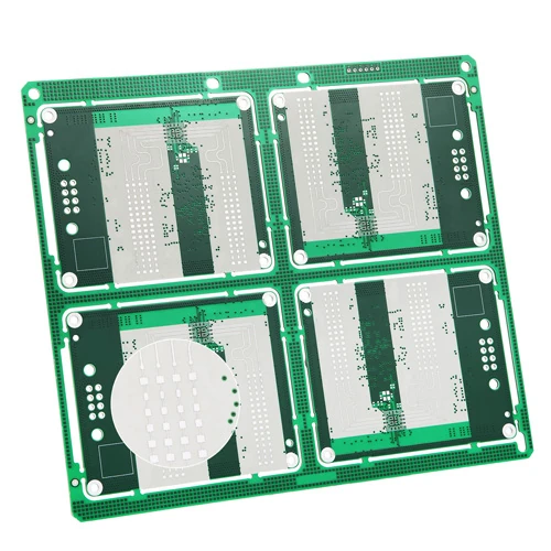
02 / RF GEOMETRY
Conductor accuracy is different from minimum conductor width.
The RF page publishes ±15 μm signal-line accuracy, interlayer alignment of ±4 mil for boards with no more than eight layers, and asymmetric-board warpage below 0.5%. The ±15 μm figure is a dimensional tolerance; it must not become a 15 μm minimum routing filter.
The listed material classes include hydrocarbon/ceramic or fibreglass, PPO with fillers, and PTFE with ceramic or fibreglass. Kinwong names mixed lamination, blind/buried/microvias and LDI. LDI is direct imaging; this statement does not identify a laser-drilling machine.
Release: exact laminate grade and thickness, copper roughness/finish, line geometry and tolerance, reference-plane stack, mixed-material press requirements, coupon geometry and the required electrical report. Agree the acceptance method for loss and impedance instead of inferring it from an antenna application.
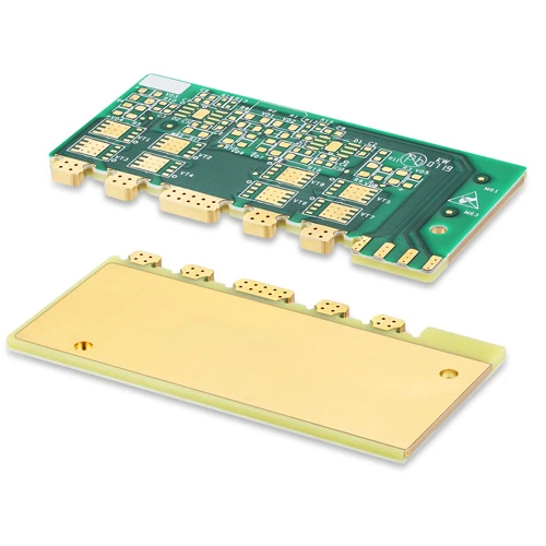
03 / EMBEDDED THERMAL INTERFACE
Dimension the insert and the circuit as one mechanical assembly.
Kinwong describes embedded copper blocks and embedded ceramics, with I, U and T-shaped blocks. Its copper-inlay table controls block size, block tolerance, height difference and clearance to conductors. Those dimensions solve a different problem from HDI routing.
Send a section drawing that identifies the insert datum, exposed faces, conductor clearance, flatness, bonding interface and inspection locations. Agree how the insert will interface with the component or cooling assembly and which measurements will appear in the shipment report.
Manufacturer-published copper-block dimensions
- Minimum block X × Y
- 5 × 5 mm
- Block Z range
- 0.5–3.5 mm
- Block X / Y tolerance
- ±50 μm
- Block Z tolerance
- ±30 μm
- Height difference
- ±30 μm
- Block-to-conductor minimum
- 0.35 mm
The 0.35 mm clearance is not minimum trace width. The table does not establish thermal conductivity, allowable current, measured thermal resistance or a qualified temperature cycle for the pictured board.
Keep rigid-zone layers and flexible-zone layers separate.
Kinwong’s rigid-flex page lists 2–16 layers in the rigid area and 1–6 in the flexible area, air-gap structures, HDI/any-layer, asymmetric 1F+1R construction and dispensing at the transition. A rigid layer maximum is not a six-layer dynamically flexing cable specification.
For a folding assembly, mark the bending region, flex thickness, bend radius, expected cycles, stiffeners and component keep-outs. For a one-time installation bend, specify that service condition explicitly. Request an approved transition and material stack before comparing quotations; the website does not provide the test conditions needed to assign a general bend-life figure to this family.
Name the production base on the approved route.
The issuer’s 2025 report identifies six Chinese production bases: Shenzhen, Longchuan, Jishui, Xinfeng, Zhuhai Jinwan and Zhuhai Fushan. It separately lists Thailand as under construction during that reporting period. A group footprint is not proof that every process is available at every base today.
Headquarters is a separate address.
The current contact page gives headquarters at No.158 Guangyuan 3rd Road, Guangming District, Shenzhen. Shenzhen manufacturing is listed at No.166 Shuiku Road, Tiegang, Bao’an. The report confirms that same distinction between office and registered address. Use the plant address, contracting legal entity and shipment origin appropriate to the quotation.
The current website’s locations page still says five manufacturing sites, all in China; Quick Facts lists seven bases including Thailand. We retain the dated issuer record and the six named contact locations rather than adding the different counts together or treating Thailand as confirmed current production. Ask for the proposed plant’s actual process availability and qualification record.
The annual report describes HLC and HDI/SLP projects at its Zhuhai subsidiary. That helps direct a technical question, but it does not assign the three catalogue photographs to Zhuhai or reserve production capacity for a new order.
Turn the published capability into a drawing-specific approval.
Kinwong’s quality page describes APQP conversion of customer requirements, supplier management, SOP-based process control, change management, traceability and outgoing inspection. Its technical page describes a central laboratory and a historical CNAS accreditation statement. Those statements are useful context; they do not establish the current accredited scope or a test report for your lot.
Before the quotation
Name the critical process and manufacturing base. Supply one controlled stack, material grades and drawing revision. For HDI, identify the microvia/build-up sequence; for RF, the electrical and dimensional acceptance; for embedded copper, the interface drawing and inspection datums.
Before production
Obtain a signed manufacturability review and agreed inspection plan. Define which cross-sections, coupons, dimensional records and material-lot records accompany delivery. If a UL or automotive approval is required, check the proposed legal entity, site, construction and certificate scope before release.
When the route changes
Agree change notification for laminate substitution, process relocation, build-up changes and outside processing. Decide which changes need renewed qualification. Keep the approved sample route and the volume route traceable to the same drawing revision.
The annual report’s application disclosures include high-current, high-layer-count and advanced HDI programmes. They do not justify combining the finest routing, highest layer count, thickest copper and tightest RF tolerance into one default directory promise.
Prepare the fabrication RFQ →Sources behind this profile
Individually researched on 8 October 2026. Original catalogue photographs illustrate named board families; process figures and dated issuer disclosures retain their own scopes. This research is not a PCBVerified factory audit or certification.
- MANUFACTURER / COMPANYCurrent Quick Facts and product families ↗
- ISSUER / 2025 REPORTIdentity (p5), application scopes (p10), sites and Thailand construction status (p11), Zhuhai projects (p4) ↗
- MANUFACTURER / HDImSAP, tenting and original HDI catalogue image ↗
- MANUFACTURER / RFDimensional accuracy, laminate classes and original RF image ↗
- MANUFACTURER / COPPER INLAYBlock dimensions, clearance and original catalogue photograph ↗
- MANUFACTURER / RIGID-FLEXRigid/flexible-zone layer scopes and transition features ↗
- MANUFACTURER / CONTACTHeadquarters, six manufacturing locations and sales contact ↗
- MANUFACTURER / LOCATIONSOlder five-site wording retained as a source discrepancy ↗
- MANUFACTURER / QUALITYAPQP, supplier management and outgoing quality control ↗
- MANUFACTURER / TECHNICALR&D and historical laboratory accreditation statement ↗