Choose the manufacturing handoff before comparing the headline limits.
KingBrother positions its business around electronic-product development: PCB engineering, prototype and small-to-medium-batch fabrication, assembly, component sourcing and testing. This profile represents 惠州市金百泽电路科技有限公司, the Huizhou PCB company. The listed Shenzhen parent’s 2025 annual report identifies this subsidiary’s principal business as PCB, separately from the group’s engineering-design and PCBA companies.
The official catalogue contains specific board constructions as well as a separate prototype/batch capability chart. That distinction is useful when a design is moving from an engineering sample to repeat supply. Choose the required construction below, then agree the producing plant, process route and acceptance records for that design.
ORIGINAL GROUP CATALOGUE / FIVE DISTINCT ROUTES
A backplane, flex interface, RF cavity and power board need different evidence.
Each photograph below is paired with its own manufacturer-labelled specifications. These are group catalogue examples; the website does not assign each example to Huizhou. Request the actual plant and a compatible, approved fabrication stack. These entries are not interchangeable combinations of the general process limits.
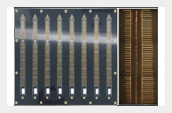
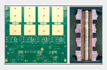
Official high-speed backplane entry: TU872-SLK, 48 layers, 5.0 mm, 4.8 / 4.8 mil.
48-layer TU872-SLK backplane
Published laminate
TU872-SLK
Layers / thickness
48 / 5.0 mm
Minimum line / space
4.8 / 4.8 mil
Start with the channel and connector interface. Send reference planes, dielectric and copper thicknesses, target impedance and the connector’s finished-hole fit. If back-drilling is needed, release the layer pairs, residual-stub requirement and measurement method rather than assuming it from a “high-speed” title. Agree material substitution and first-article coupon results for this particular stack.
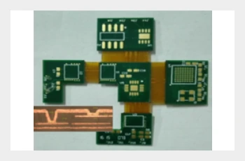
Second-order HDI + rigid-flex; medical application in the source.
8-layer HDI rigid-flex · 1.2 mm
Line / space
3.0 / 3.0 mil
Source hole-depth notation
0.12 mm; cross-layer drilling process
The 0.12 mm value is labelled hole depth, not finished-hole diameter. Define the actual via sequence, dielectric thicknesses, copper interfaces and flex transition. Ask how the proposed build-up is qualified, which microsections are supplied and which bend condition applies. A medical-use catalogue label does not specify the buyer’s regulatory or reliability acceptance.
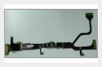
Release the rigid and flexible zones separately. Identify the shielding-film grade, grounding method, adhesive stack, coverlay openings and the termination interface. Specify static installation or repeated movement, bend location and acceptance. Ten flex layers and a shielding film do not establish a universal bend radius or EMI result.
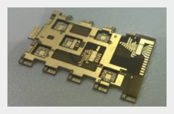
Mixed-lamination high-frequency stepped board; three stepped-groove operations.
RO4350B + S1000-2 · 8 layers
The source gives 1.5 mm board thickness and “three stepped grooves.” It does not give their depth tolerances, a loss measurement or an impedance value. Supply the layer-specific material map, bonding sequence and a dimensioned cavity section with datum and remaining-dielectric requirements. Agree the coupon and material-lot evidence where RF performance governs acceptance.
Power application: four layers, 2.4 mm, inner and outer copper 12 oz, 20 / 20 mil.
12 oz copper · power-board construction
Define whether the quoted copper is starting foil or required finished copper; the catalogue does not resolve that distinction. Supply etched conductor dimensions, connection geometry and thermal requirements for the actual operating condition. Agree copper and hole-wall measurements, solder-mask coverage and the stack approval. Current rating cannot be read from copper weight alone.
MANUFACTURER CAPABILITY IMAGE / PROTOTYPE AND BATCH
Move the design into the batch column before scaling an order.
The official PCB capability chart has separate 样板 (prototype) and 批量 (batch) columns. The following figures are transcribed from that chart, rather than taken from the CAD-design page or assigned to a photographed board. The chart is undated and group-level.
Prototype column
FR-4 layer maximum
68
Rigid-flex total / flex layers
28 / 16
HDI
28 layers / fourth order
Line / space minimum
2.0 / 2.0 mil
Maximum thickness / copper
12 mm / 18 oz
Mechanical / laser hole minimum
0.10 / 0.10 mm
Published aspect ratio
20:1
Impedance control tolerance
±5%
Batch column
FR-4 layer maximum
28
Rigid-flex total / flex layers
20 / 12
HDI
20 layers / third order
Line / space minimum
3 / 3 mil
Maximum thickness / copper
6.5 mm / 6 oz
Mechanical / laser hole minimum
0.15 / 0.10 mm
Published aspect ratio
16:1
Impedance control tolerance
±10%
The hole rows are labelled mechanical and laser holes, without explicitly defining finished plated diameters. Keep that definition open in the enquiry. The chart also lists high-frequency mixed lamination at 28 prototype / 20 batch layers and pure PTFE at 24 / 16 layers. Delivered dimensions are up to 550 × 900 mm in the prototype column and 550 × 620 mm in the batch column.
Resolve a source difference before placing repeat work.
The group’s 2025 annual report describes a different headline range: up to 64-layer PCB and up to 30-layer any-layer HDI. Those dated group statements and this undated chart should not be merged into one maximum specification. Ask for the current plant-specific process chart and an engineering decision on the proposed construction.
For the 48-layer and 12 oz catalogue examples above, ask what repeatable lot size and production route are offered: those figures exceed the corresponding FR-4 layer and copper maxima in the chart’s batch column. This is a question about qualification and scope, not proof that the catalogue is false or that a prototype automatically scales.
OPTIONAL DOWNSTREAM HANDOFF
PCB manufacture, assembly and functional acceptance are separate releases.
Fabrication release
Approve the stack, drill and via definitions, laminate grades, copper, finish zones and mechanical datums. Identify the producing entity and the first-article records. Specify the revision used for electrical testing and how substitutions are approved.
Assembly release
If assembly is included, send the BOM with approved alternates, placement data, assembly drawings, polarity and special handling instructions. The group’s EMS table distinguishes a routine 0201 package from a non-routine 01005 package; routine QFP and BGA pitch is 0.4 mm, with 0.3 to below 0.4 mm in the non-routine column. Check the actual board, component height and equipment assignment together.
Test release
Agree fixtures, programming, coverage, limits and ownership of the test procedure. The group website describes environmental and reliability testing and failure analysis, including thermal shock, vibration, microsections, SEM/EDS, X-ray and C-SAM. Obtain the relevant lab, method, sample quantity and reporting scope for the order; a list of test services is not a passing result.
Ask which party supplies components, builds the assembly, operates the test and owns disposition of failed boards. The 2025 report lists separate PCBA subsidiaries, so an integrated group quotation should still identify the entities performing each step. No equipment model, lab accreditation scope or installed Huizhou assembly line is inferred here.
HUIZHOU / ORDER QUALIFICATION
Make the manufacturing address part of the approval.
The official contact page names the Huizhou production base at Longshan Sixth Road, south of Banzhangling, Xiangshuihe Industrial Zone, Daya Bay, Huizhou. It also lists a separate Xi’an production base and other group offices or production locations. Use the named Huizhou legal entity and the actual plant address in the quotation, qualification package and change-control agreement.
The manufacturer’s qualifications page lists ISO 9001, ISO 14001, ISO 45001, ISO 13485, IATF 16949 and lab-related claims, as well as UL/CQC/CCC references. That page does not provide the holder, expiry and precise scope needed to qualify this Huizhou order. Request current issuer records and, where applicable, the exact UL file, material construction and production-site coverage. This profile does not display an active certification or UL-ownership badge on that basis.
The first enquiry should lead to a plant-specific answer.
Select the closest construction above, identify whether the requirement is a prototype or a recurring build, and attach the released stack and critical acceptance features. Ask the factory to return the manufacturing site, combined process approval, material substitutions, lot size and the records supplied at delivery. Keep group engineering or assembly services explicit additions to the bare-PCB scope.
SOURCE TRAIL
Sources behind this profile
Individually reviewed 8 October 2026. Five original catalogue photographs, the two capability images and the issuer report were read separately. Catalogue and process-chart information is group-level; Huizhou is the PCB entity represented here. Buyer release guidance is editorial analysis, not a factory test result.