

MANUFACTURER DOSSIER
Jove PCB
深圳中富电路股份有限公司 · Guangdong
Company facts at a glance
- Chinese legal name
- 深圳中富电路股份有限公司
- English name
- Shenzhen Jove Enterprise Limited. “JOVEPCB Enterprise Ltd”, used on the English website, is the Hong Kong subsidiary.
- Short names
- 中富电路 · JOVE
- Listing
- Shenzhen Stock Exchange ChiNext, 300814, listed 12 August 2021
- Founded
- 12 March 2004
- Registered address and main plant
- No. 8 Xingye Road, Shajing Subdistrict, Bao’an District, Shenzhen
- Other plants
- Songgang branch plant, Shenzhen; Heshan, Guangdong, run by subsidiary 鹤山市中富兴业电路有限公司 (No. 59 Chuangli Road); Rayong, Thailand, run by WTT Electronics Co., Ltd., in mass production since 2025
- Capacity
- The 2025 annual report gives output and sales in RMB only. The latest area figures are from the 2021 prospectus: 949,000 m² capacity and 759,600 m² output in 2020.
- Process capability
- Website: multilayer up to 34 layers for samples and 24 in volume, any-layer HDI up to 14 layers, about 40 µm line and space, rigid-flex 2 to 24 layers
- Management systems
- ISO 9001, ISO 14001, ISO 45001, QC 080000, IATF 16949, ISO 13485, ISO 27001 and ISO 50001, as listed in the 2025 annual report without numbers or dates
- UL files
- E232940 (printed wiring boards, ZPMV2) and E468708 (flexible, ZPXK2), held by Shenzhen Jove Enterprise Ltd
Checked on 29 October 2026 against the 2025 annual report and 2021 listing documents on CNInfo, the official website and UL iQ for Printed Wiring Boards. The website’s About page still describes three bases with Thailand as planned.
Start with the electrical and mechanical job.
Jove is the brand of 深圳中富电路股份有限公司, the Shenzhen-listed PCB manufacturer identified as stock 300814 in its 2025 annual-report summary. Its portfolio includes multilayer, rigid-flex, HDI, metal-base and RF antenna boards. The useful distinction for a buyer is the manufacturing route: a moving flex connection, a power conversion stack and an antenna interface need different drawings, copper rules and acceptance tests.
The photographs below are original official product-family images. They show the families Jove presents; the technical tables describe process ranges rather than measured specifications of the pictured boards. The quoted figures remain attached to their source column, copper condition and hole definition.
One assembly, two mechanical environments.
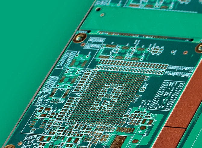
The overview describes total constructions of 2–24 layers with a 1–6-layer flex region, symmetric or asymmetric flex-layer arrangements and possible dynamic-bend designs. The distinction matters: total board layers are not flex-region layers, and a rigid section’s copper schedule cannot simply continue through the bend.
- First detailed table / sample column
- Maximum 18 layers
- First detailed table / volume column
- Maximum 24 layers
- Outer 3 oz routing / both columns
- 8 / 11 mil line / space
- Inner 2 oz routing / both columns
- 6 / 5.5 mil line / space
The headline’s 40/40 µm statement is a separate fine-line claim. The detailed table conditions inner-layer routing on copper: at ⅓ oz it lists 2/2 mil sample and 1.5/1.5 mil volume, while outer ⅓ oz routing is 3/3 mil in both columns. These entries cannot be combined with 3 oz outer copper to quote an exceptionally fine, heavy-copper bend.
Keep the second table identifiable
The page repeats the Chinese heading “rigid-flex technical parameters” above a second table containing coverlay, reinforcement, air-gap and laser/punch-outline entries. That table lists 6 sample / 8 volume layers, coverlay registration ±0.15 / ±0.10 mm and reinforcement registration ±0.20 / ±0.15 mm. Preserve its identity when asking engineering which table applies to your flex construction; do not replace the overview’s 1–6 flex-layer range with the larger table value without confirmation.
Release the rigid-to-flex boundary, adhesive/adhesiveless laminate choice, copper orientation, coverlay openings, stiffener drawing and connector mating thickness. For repeated movement, state bend radius, travel, duty cycles, temperature and how an assembled test coupon will represent the actual installation. The site mentions UL-qualified laminate combinations, but does not provide a file number on this page; an order still needs the applicable holder, construction and file scope.
The 34-layer headline includes a sample route.
Jove’s multilayer page describes energy products, planar transformers, embedded passives and copper-block thermal constructions. Its detailed table explicitly separates volume production from samples. That distinction is more useful for qualification than the single maximum-layer headline.
Volume column
- Maximum layers
- 24
- Inner / outer copper range
- ½–6 oz
- Inner 6 oz line / space
- 14 / 14 mil
- Outer 6 oz line / space
- 16 / 16 mil
Sample column
- Maximum layers
- 34
- Inner / outer copper range
- ½–12 oz
- Inner 6 oz line / space
- 12 / 12 mil
- Outer 6 oz line / space
- 14 / 14 mil
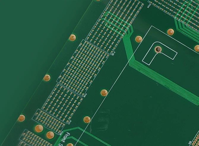
For a power converter or planar transformer, give winding topology, layer copper, dielectric insulation, terminal connections and the required isolation test. The table lists testing voltage maxima of 6,000 V DC / 5,000 V AC for volume and 10,000 V DC / AC for samples. Those are factory test-capability entries, not the working-voltage or safety rating of a delivered design; agree test duration, ramp, leakage criterion, coupon and applicable insulation requirements.
Back-drilling has its own conditions: volume diameter 0.4–1.0 mm with D+0.2 mm enlargement; sample diameter 0.4–6.35 mm with D+0.15 mm. Listed stub ranges are 0.05–0.25 mm volume and 0.05–0.20 mm sample. Release the reference plane, target layer, residual-stub measurement and protected layers together. The page’s general ±8% impedance headline differs from the detailed table’s ±10% volume / ±7% sample for differential impedance and single-ended targets ≥50 Ω. Use the negotiated order specification.
Specify how the microvia reaches its target.
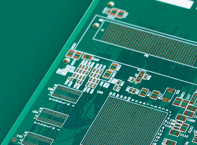
The narrative supports 1+N+1 through any-layer HDI and mentions 14-layer any-layer functionality. The detailed chart has two identically labelled “specific capability” columns. It gives 4–24 versus 4–34 layers, up to five versus six lamination cycles, and first-column 1-N-1 / 2-N-2 / 3-N-3 versus second-column 4-N-4 and ELIC (12L) in addition. These columns are not labelled volume and sample. Ask Jove to identify the applicable process class rather than assigning the best values to all production.
- Minimum inner line / space
- 50 / 50 µm · 40 / 40 µm
- Minimum outer line / space
- 60 / 60 µm · 50 / 50 µm
- Laser-hole entries
- 75 µm · 50 µm
- Filled-laser-hole aspect ratio
- ≤0.8:1 · ≤1:1
Keep the left/right entries separate. The process-specific inner-line rows also pair “1.4 mil” with “40 µm” and “1.2 mil” with “35 µm”; the published unit pairs are not exact conversions. Ask engineering to issue one controlling dimensional unit. Minimum mechanical-drill entries of 0.20 and 0.15 mm are drill-bit dimensions, not finished plated holes.
Send the build-up drawing, stacked or staggered via arrangement, dielectric thickness by lamination, target lands and the required fill/cap construction. Request the microsection and reliability acceptance relevant to that construction. The overview mentions plated copper or copper-paste filling and thermal-management options; it does not establish that every fill route, embedded copper and finest routing can be made simultaneously.
Antenna manufacture needs its own release sheet.
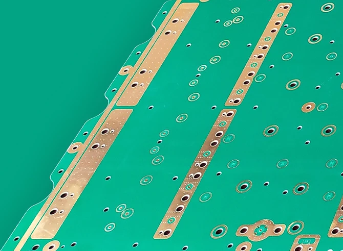
Jove lists phase-shifter, sliding-contact, divider, calibration and other base-station antenna boards. The standard column covers single/double/three-layer boards and 0.2–2 mm thickness; the advanced column lists four, six and seven-or-more layers with 2–6 mm thickness. Its narrative separately describes delivered seven-layer 5G antenna boards. Treat that historical example and the general column as different scopes.
- Plated line / space tolerance
- Standard ±1.5 mil / advanced ±1.0 mil
- Outline and slot tolerances
- Standard ±0.10 mm / advanced ±0.075 mm
- Specified PIM test bands
- 800 / 2100 / 2600 MHz
- Named test instrument
- Rosenberger
The table reports average PIM thresholds ≤−115 dBm (158 dBc) standard and ≤−117 dBm (160 dBc) advanced. These units are not interchangeable without the carrier conditions. Include carrier frequencies and powers, order of intermodulation, fixture, connectors, calibration, contact condition and acceptance statistic. They are process-chart claims, not an attached test report for the photographed board.
The material list includes Shengyi PTFE and PPE systems, Rogers RO4730G3 and other supplier grades. One multilayer row places RO4730G3+RO4450F and NYHP7300+NY6300 under a single supplier label; verify each laminate/bonding-sheet manufacturer and grade separately. Obtain the actual lot trace and stack-up. Standard/advanced thicknesses, maximum lengths and test bands do not establish a fully qualified combination for your antenna.
Name the plant on the engineering release.
The company introduction names Shajing and Songgang in Shenzhen and Hecheng in Heshan, Jiangmen, while still describing a planned Thai base. A newer original investor-relations record, dated 7 May 2026, discusses orders entering the Thailand factory and a stronger AI-power focus at Jiangmen. The older introduction therefore does not describe the full newer operating picture. Ask for the proposed fabrication entity, plant and route on the quotation; the global sales map mixes offices, agents and factories.
Before a quotation
Identify rigid-flex, HDI, power or antenna manufacture; send the actual stack, copper conditions, dimensions and quantity. Ask which published table and column governs the build.
Before qualification
Agree sample-to-volume changes, fabrication site, approved material list and certificate holder/scope. The quality page’s management programmes do not substitute for a current scoped certificate.
Before shipment
Request the drawing revision, netlist test, applicable impedance/PIM/isolation results, hole and microsection records, material lots and approved deviations belonging to this batch.
The official contact page separates business enquiries from investor relations and supplier procurement. A sales-office address is not automatically the manufacturing location. Keep the factory assignment and engineering contact in the PCBVerified RFQ conversation alongside the returned DFM and acceptance record.
Sources behind this profile
Reviewed 8 October 2026. Official product-family photographs and process tables are kept separate. Issuer filings establish the dated corporate record and reported plant direction; they do not independently certify the pictured boards or any combined manufacturing extreme.
- Official companyJove company introduction ↗
- Official processRigid-flex and flex tables ↗
- Official processMultilayer and power process table ↗
- Official processHDI structures and two-column chart ↗
- Official processAntenna materials and PIM table ↗
- Official contactBusiness, procurement and investor contacts ↗
- Issuer filing2025 annual-report summary, 29 April 2026 ↗
- Issuer filingFactory positioning and AI-power discussion, 7 May 2026 ↗
- Official qualityManagement and named plant personnel ↗