Approve the board construction before starting the quick-turn clock.
JCL PCB · 深圳市聚创立电子科技有限公司 publishes prototype and small-to-medium-batch fabrication, with plated half-holes, thick boards, heavy copper and blind/buried vias among its specialist routes. The company also offers PCB assembly. Its catalogue makes the distinction concrete: four-layer Bluetooth boards, a third-order eight-layer automotive board, metal-edge headset boards and thick-copper medical-instrument boards.
BARE-BOARD RELEASE
Stack, holes and finish
Confirm the electrical layers, sequential-lamination route, finished copper and plated-hole definitions against one drawing revision.
The assembly page starts its lead-time statements after all materials are ready. Component shortages and engineering approval need separate milestones.
The company page advertises 48-hour multilayer prototypes, 72-hour small batches and 8-/12-hour rush options. Treat these as routes to request, subject to file review, construction and allocation. An assembled, inspected shipment needs its own written completion date.
THREE DIFFERENT SPECIAL-PROCESS QUESTIONS
HDI, edge metal and heavy copper need different drawings.
Eight-layer automotive control board: third-order route
Catalogue construction
8 electrical layers; title says third order
Finish / mask
Immersion gold / green
Application
Automotive control
Request the sequential-lamination stack, blind/buried via map and filled/capped-via acceptance. Automotive use in a catalogue is not an IATF or automotive qualification statement.
Four-layer headset PCB with metal edge wrapping
Catalogue construction
4 electrical layers
Finish / mask
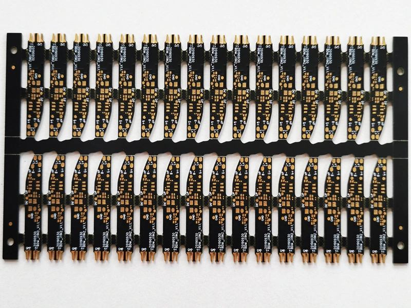
Immersion gold / matt black
Special feature
Metal edge wrapping, as titled
Specify exactly which edges need metallisation, its continuity, thickness and clearance from circuitry. Metal edge wrapping and castellated holes need separate manufacturing drawings.
Four-layer thick-copper medical-instrument board
Catalogue construction
4 electrical layers; thick copper
Thickness wording
Title says 4.0 board thickness; no unit attached
Application
Medical instrument
Confirm board thickness in mm and finished copper in oz or micrometres. The catalogue title supplies no copper weight, medical-device approval or patient-safety validation.
FOUR- AND SIX-LAYER CATALOGUE CONSTRUCTIONS
Compare the actual board examples, then specify the signal requirements.
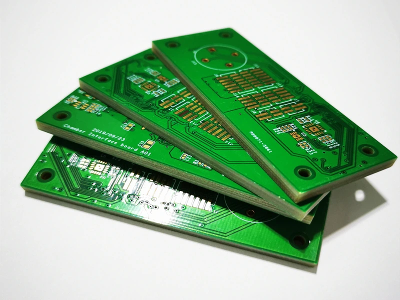
These photographs are paired with their individual official product pages. Layer counts and finish names below come from the corresponding titles. USB, Bluetooth, camera and scanner applications do not by themselves supply an impedance tolerance or a functional-test result.
Four-layer Bluetooth-module PCB
Catalogue construction
4 electrical layers
Finish / mask
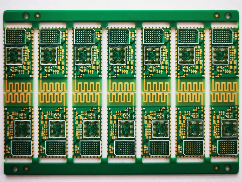
Immersion gold / green
Application
Bluetooth module
Specify the laminate, controlled-impedance lines and panel breakaway. The Bluetooth title does not provide a measured RF loss or approved radio-module performance.
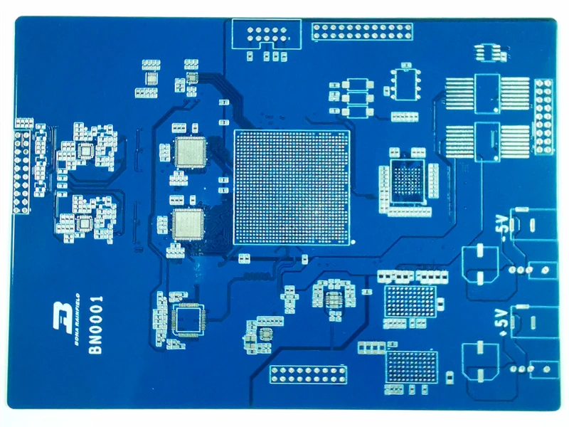
Six-layer communications mainboard
Catalogue construction
6 electrical layers
Finish
Tin spray; lead content unspecified
Mask conflict
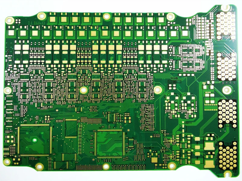
Title says green; corresponding photograph is blue
Put the actual mask colour, finish chemistry and lead-free requirement on the drawing. Ask which artwork revision the illustrated mainboard represents.
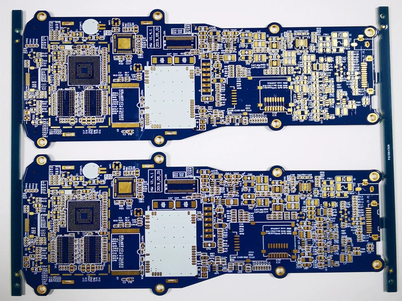
Six-layer handheld-scanner mainboard
Catalogue construction
6 electrical layers
Finish / mask
Immersion gold / blue
Application
Handheld scanner
Submit the actual connector, assembly-rail and flatness requirements. The example gives no numerical trace, plated-hole or impedance tolerance.
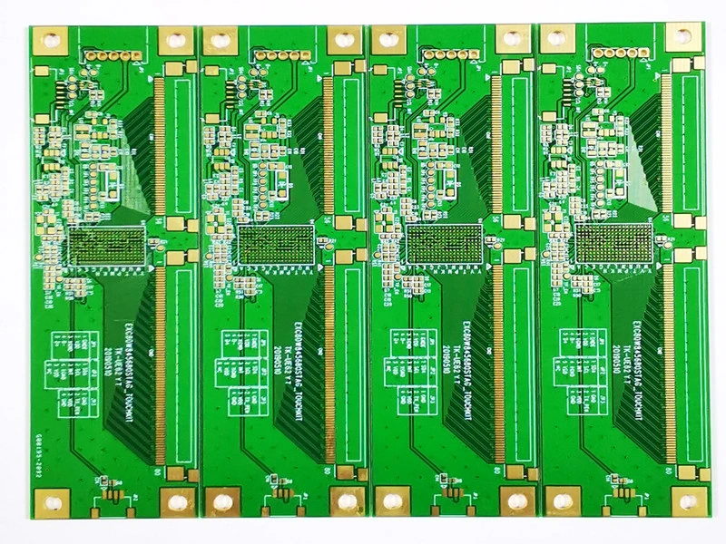
Four-layer camera mainboard
Catalogue construction
4 electrical layers
Finish / mask
Immersion gold / green
Application
Camera mainboard
Provide the camera connector and any controlled-impedance differential-pair requirements. Neither image nor application title establishes signal-integrity acceptance.
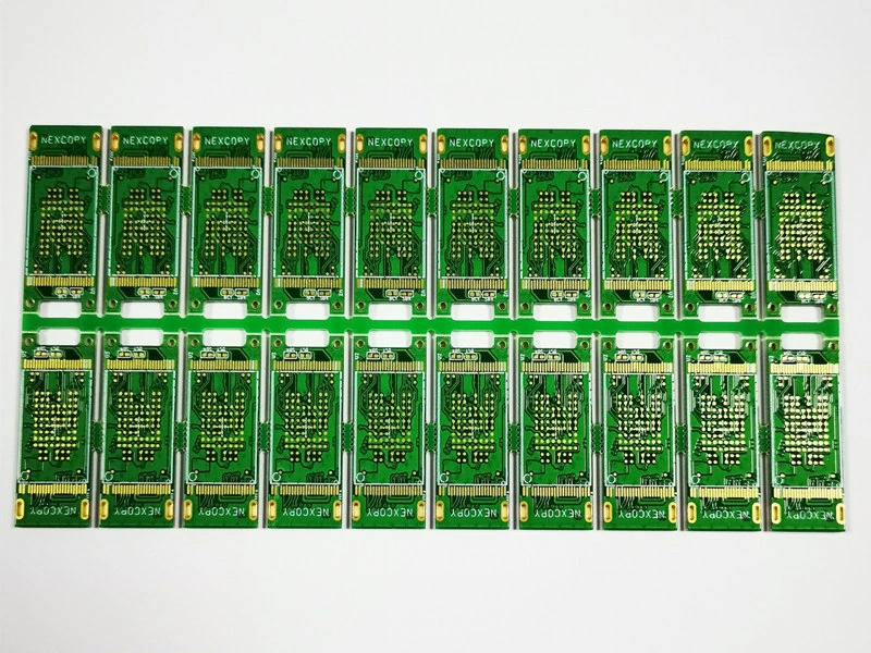
Four-layer USB-device board
Catalogue construction
4 electrical layers
Finish / mask
Immersion gold / green
Application
USB device
Specify the USB generation, impedance target, connector plating and assembled-board test. This bare-board example does not establish USB protocol compliance.
PUBLISHED PROCESS TABLE / ROUTINE AND CONDITIONAL VALUES
Use routine geometry first; escalate special conditions to engineering.
Patterning and stack
Electrical layer range
1–24; through, blind/buried and half-hole routes listed
Routine trace / space
4 mil / 4 mil
Conditional minimum
3 mil, also printed as 0.075 mm; requires the stated special conditions
Board thickness
0.2–8 mm; stack and special material procurement govern availability
Thickness tolerance
≥1 mm: ±10%; below 1 mm: ±0.1 mm
Finished copper
Outer 35–210 μm / up to 6 oz; inner 18–140 μm / up to 4 oz
The table calls for geometry review above 3 oz inner copper. Specify the copper distribution by layer; its finest pattern and heaviest copper entries are not evidence of an achievable combination.
Hole definitions and impedance
Mechanical drill minimum
0.15 mm; 0.2 mm described as routine
Laser drilling
0.10 mm identified for the HDI route
Mechanical finished-hole range
0.20–6.5 mm
Half-hole minimum
0.5 mm; separate from a via drill size
Annular-ring entry
≥0.153 mm / 6 mil, with dense geometry subject to review
Impedance entries
±5 Ω and ±10%; no target-range mapping supplied
The process page uses ±0.05 mm and a finished-hole example, while the homepage FAQ separately states ±0.075 mm for PTH and ±0.05 mm for NPTH. Put finished PTH and NPTH dimensions and tolerances on the drawing and request approval of any exception.
Two panel-size statements need a route-specific answer.
600 × 400 mmMaximum-size headline in the process table
520 × 415 mmIts separate regular-size statement
One dimension in the “regular” entry exceeds the corresponding maximum entry. Ask for usable panel dimensions, orientation, rails and finished-board size for your selected construction. Do not select the larger value independently on each axis.
Artwork details that can change acceptance
Panel gaps: the table distinguishes zero-gap panels from routed gaps of at least 1.6 mm; trace clearance is ≥0.3 mm from a routed edge and ≥0.4 mm from the V-score centre.
Mask: the 0.2 mm statement concerns IC-pin spacing at which bridges are offered. It should not be entered as a guaranteed 0.2 mm mask-bridge width.
Gold fingers: bevel 45° ±5° and remaining thickness 0.5 ±0.13 mm are separate drawing features. Immersion-gold thickness is listed as 1–3 μin; contact finish needs its own specification.
File authority: provide one controlling outline, drill/slot definitions and the correct solder-mask layers. Paste layers still matter for a separate stencil or assembly order.
Material: FR-4 brands listed include Shengyi, Nanya, Kingboard and Guoji. Request the actual grade, stack and batch documentation. The metal-board “1.0 W” wording lacks the full thermal-conductivity unit, so it is not treated as a validated W/m·K rating.
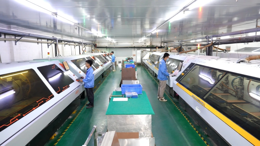
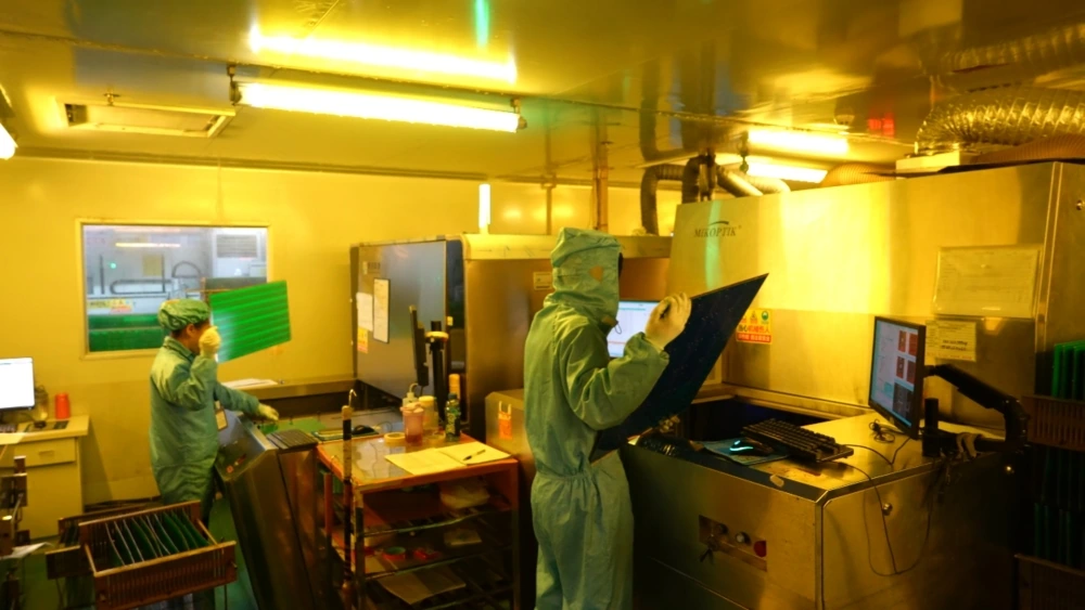
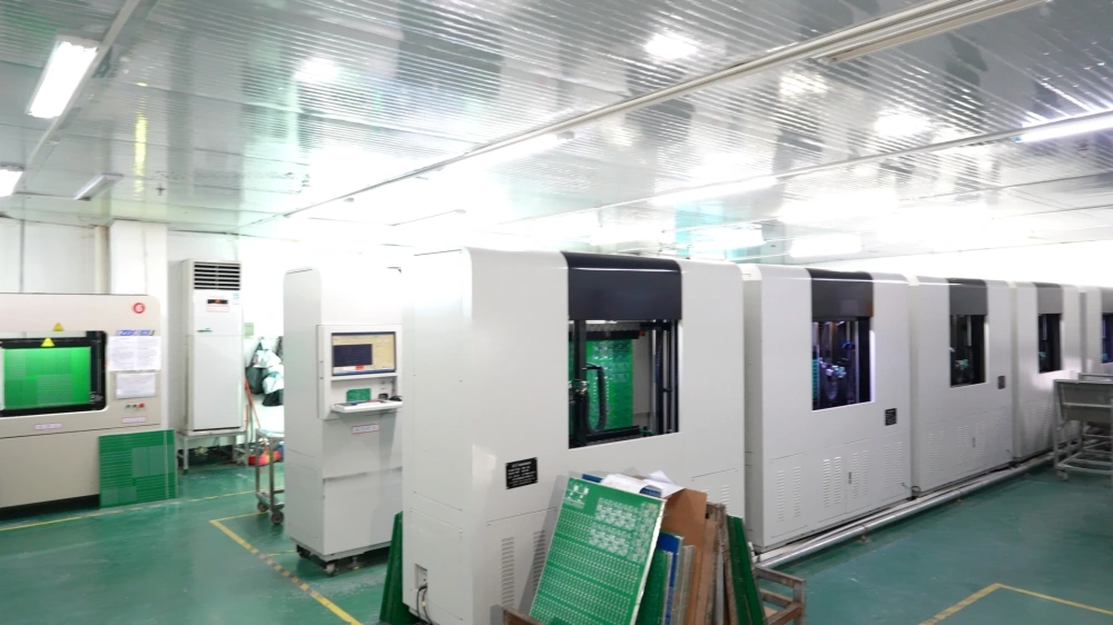
The same factory gallery labels solder-mask LDI, vacuum etching, pulse plating, automatic copper deposition, AOI, electrical testing and CNC profiling. These are manufacturer-labelled process photographs. Ask which site performs the special step, which netlist/coupon is tested and which records ship with your boards.
PASTE PRINTING → PLACEMENT → REFLOW → INSPECTION
The panel has to fit every stage of the assembly route.
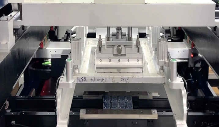
PRINTING50 × 50 to 400 × 340 mm
The automatic paste-printer entry. Smaller bare boards may need a panel; agree rail and stencil dimensions.
PLACEMENTUp to 1200 × 460 mm
The Yamaha-machine entry, not a demonstrated maximum for the complete production line.
SERVICE TABLE45 × 45 to 450 × 1200 mm
The separate PCBA-service statement; it needs reconciliation with the printer and panel route.
For a large board, request the actual printing method, carrier, placement orientation, reflow support and inspection plan. The larger placement-machine figure cannot override the smaller printer limit without an agreed alternative process.
Placement and soldering
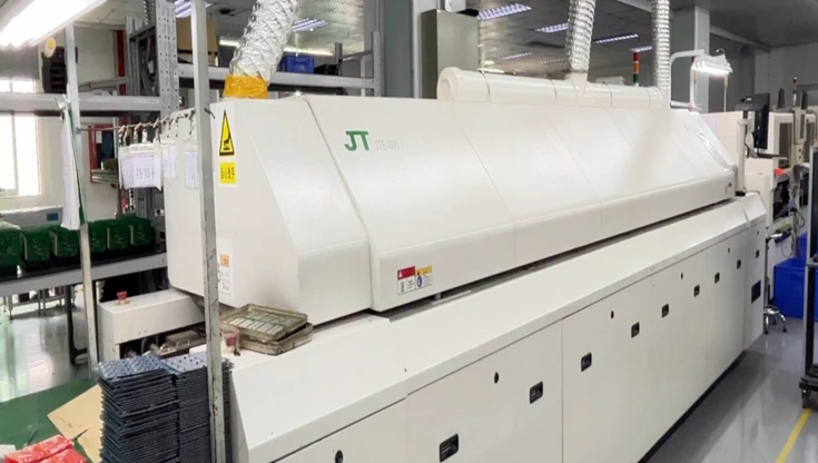
The PCBA page explicitly uses imperial 01005 (0.4 × 0.2 mm) and also lists 0201. It states 37.5 μm / 0.0375 mm placement accuracy and describes a JT reflow oven with ten upper and ten lower zones. Its 0.25 mm BGA-pitch statement concerns X-ray inspection; it is not a supplied placement-yield or functional-test report.
Supply a controlled BOM, approved substitutions, placements, assembly notes and the agreed stencil/panel revision. The service offers full component sourcing, partial sourcing and assembly-only arrangements; identify ownership of shortages and customer-supplied parts.
Inspection and shipment
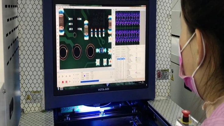
The page describes AOI for wrong/missing/reversed/offset components and related assembly defects, plus first-article and in-process checks. Request the coverage and results required for your project. An AOI image does not establish functional operation; include your power-up, firmware and test-fixture procedure if those outputs are needed.
The published schedule is 3 days for samples up to 50 pieces, 5 days for 50–500 and 7 days for ≥500, after all materials are ready. The bands overlap at 50 and 500; ask which band applies. Confirm engineering release, all-materials-ready date, assembly completion and shipment separately.
Automatic paste printer shown on the PCBA pageJT reflow equipment shown on the PCBA pageAssembly AOI inspection shown on the PCBA page
Attach a release package that answers this factory’s open questions.
Fabrication revision, layer stack, copper, finished holes, special edge/via drawings and laminate grade.
Panel size including rails, printer-compatible route, paste files, BOM and placements.
Controlled-impedance targets, coupons, bare-board netlist and required assembly inspection/functional records.
Contracting entity, named Huizhou producing site, any external process and actual material-ready/shipment dates.
Name the company and production department on the quotation.
Shenzhen office
The current contact page gives Floor 6, Building 4, Jindi Kaixuan Plaza, No. 31 Longcheng Avenue, Longgang. The older published certificates instead use Room 806, Longnian Building, No. 29 Longcheng Avenue. The dates and addresses should not be merged.
Huizhou production departments
The website separately lists Building 3, Floor 1, Jianshi Industrial Park, Pushang Village, Longxi, Boluo and Building 1, Huachuang Industrial Park, Bailianhu Village, Longxi. Ask which department makes your stack and where assembly/inspection occurs.
Read the scope and dates on the published document copies
Business licences: the website displays separate Shenzhen and Huizhou entities. They are manufacturer-published copies; confirm the entity actually issuing your order and invoice.
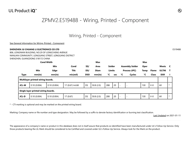
UL copy E519488: the displayed Product iQ extract is last updated 11 January 2021 and names SHENZHEN JU CHUANG LI ELECTRONICS CO LTD at the old No. 29 address. JCL-M multilayer and JCL-D single-layer types are listed. No current issuer lookup or Huizhou-site coverage was established here; the extract itself says appearance in the database does not assure a particular product was made under UL follow-up service.
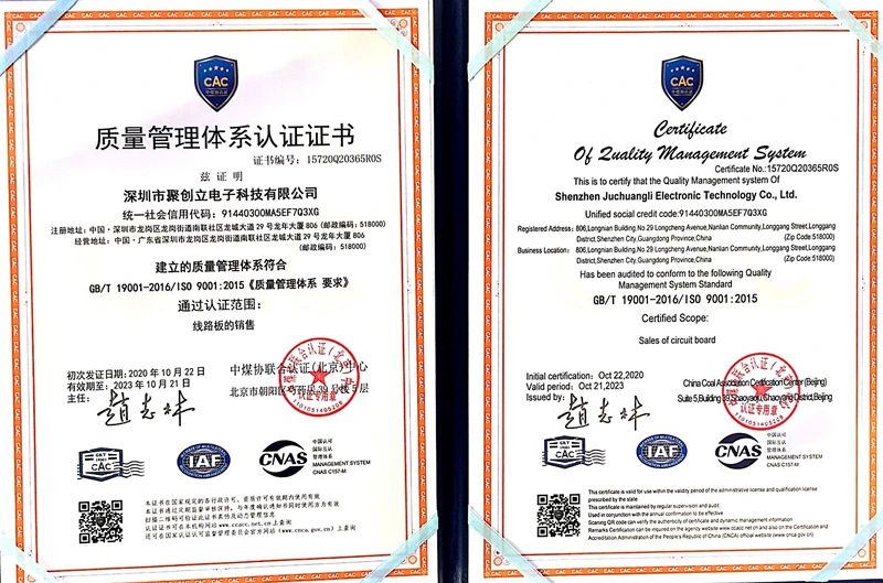
ISO 9001: copy 15720Q20365R0S covers sales of circuit board, for the Shenzhen entity; 22 October 2020 to 21 October 2023. It is not a current fabrication-site certificate.
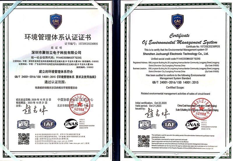
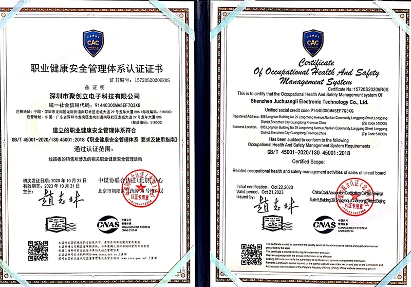
ISO 14001 / 45001: copies 15720E20236R0S and 15720S20206R0S cover environmental and occupational-health/safety activities related to circuit-board sales, with the same dates. Ask for any renewed certificate and its actual scope.
Historical manufacturer-hosted UL Product iQ extractPublished ISO 9001 copy: PCB sales scope, expired 2023Published ISO 14001 copy: sales-related scope, expired 2023Published ISO 45001 copy: sales-related scope, expired 2023
The contact page publishes 18617161557@163.com and +86 199 2458 1330. These are website contact records; no mailbox-control test or outgoing message was performed. Select a construction above to keep your enquiry within PCBVerified.
SOURCE TRAIL
Sources behind this profile
Individually researched 9 October 2026: complete original pages, eight paired catalogue photographs, labelled factory and assembly images, published certificate copies and the original CNIPA notice. Missing sample geometry remains unknown. Mask colour, panel dimensions, hole tolerances and document scope are explained at the relevant decision; no generic limits were assigned to the pictured boards.