MANUFACTURER DOSSIER

Huihe Circuit

Official sources reviewed2026-10-08
HUIHE / SPECIAL CONSTRUCTIONS FROM XINFENG

Choose the manufacturing route before comparing a layer count.

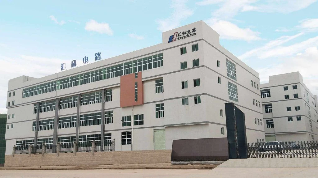
Huihe Circuit identifies its manufacturing base as Xinfeng Huihe Circuits Co., Ltd. · 信丰汇和电路有限公司, at Building 2, Xinda Industrial Park, Lvyuan Avenue, Xinfeng County, Ganzhou, Jiangxi. Its catalogue spans conventional multilayer boards, castellated edges, filled vias, RF mixed laminates, heavy copper and rigid-flex. These processes solve different assembly problems and need different release information.

The company reports a 12,000 m² workshop and 35,000 m²/month PCB capacity. These are manufacturer statements, rather than a measurement of today's available production slots. Its introduction says 2–30 layers; the detailed rigid process table instead separates 1–20-layer volume work from 2–28-layer samples. Ask which route and acceptance conditions apply to the quoted board.

A September 2026 Xinfeng County government recruitment notice names this legal entity at Xinda Industrial Park and lists CAM, plating, solder-mask and routing roles. It provides a dated local identity record, not a quality audit or confirmation of a machining limit.

Huihe manufacturer's posted photograph of its Xinfeng building
Manufacturer's own facility photograph. The posted company and qualification addresses identify Building 2.
ASSEMBLY INTERFACES / EDGE CONNECTIONS & FILLED VIAS

A plated board edge and a filled pad need different drawings.

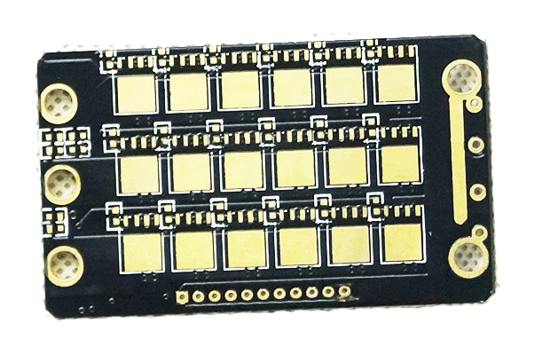
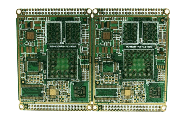
Huihe six-layer castellated PCB original catalogue panel
Six-layer castellated construction · original photograph and adjacent specification.

Six-layer castellated FR-4 board

Thickness / finish
1.2 mm / ENIG
Outer trace / space
4 / 4 mil
Inner trace / space
4 / 3.5 mil
Hole notation
0.2 mm minimum; finished status unspecified

Release the edge outline, castellated hole positions, copper keepouts and mating-board solder land together. Huihe asks for the mechanical outline to pass through each half hole. Agree edge plating, burr inspection and the retained pad after routing.

The page's separate general half-hole guide gives a 500 µm minimum diameter and 900 µm pad. That is not substituted into this example's 0.2 mm hole field: identify which holes are edge castellations and which are internal vias.
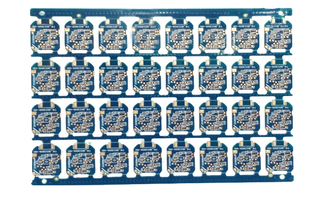
Huihe six-layer resin-filled via-in-pad original delivery panel
Six-layer resin-plugged via-in-pad construction.

Six-layer resin-filled pad construction

Material / finish
FR-4 / ENIG
Thickness
2.0 mm
Inner & outer trace / space
4 / 3.5 mil
Hole notation
0.25 mm minimum; not labelled finished

Specify which pads require resin filling, planarisation and copper capping. Agree acceptable depression, protrusion and void inspection beneath the assembly pads. The photograph alone cannot establish that these inspection conditions were met.

Huihe also shows a 0.8 mm six-layer electroplated-fill board and a 2.0 mm ten-layer electroplated-fill board. Its process table distinguishes IPC 4761 Type VII options from a special unclassified option. Ask which option applies; resin filling and copper filling are not interchangeable quotation lines.

RF / MIXED LAMINATES & PTFE

Buy a specified stack, not a list of laminate brands.

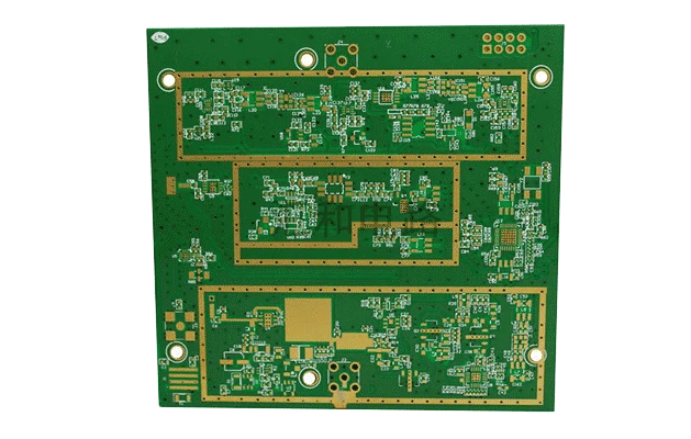
Huihe six-layer Rogers and FR-4 mixed-laminate catalogue board
Six-layer Rogers 4350 + FR-4 catalogue example.

Six-layer Rogers + FR-4 mixed stack

The accompanying specification says Rogers 4350 + FR-4, 2.3 mm thickness and ENIG, with 7/7 mil outer and 5/5 mil inner trace/space, and a 0.6 mm minimum-hole notation. It does not supply a controlled-impedance target, measured loss or a finished-hole tolerance.

Request the exact laminate grade suffix, dielectric thicknesses and bonding materials for each layer. Name the RF reference planes, design frequency, coupon method and accepted impedance or insertion-loss limits. This mixed stack is different from the second catalogue example, which specifies Rogers 3003 + FR-4 and 2.0 mm thickness.

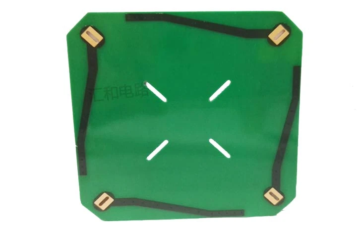
Huihe original two-layer F4BM PTFE circuit board
Two-layer F4BM PTFE example · original catalogue photograph.

Two-layer F4BM PTFE

This example specifies 0.8 mm thickness, 1/1 oz finished outer copper and lead-free HASL. The source gives Dk 2.35 and a 0.3 mm minimum-hole field, but does not attach a measurement frequency or method to that Dk figure.

Agree the full F4BM grade and supplier lot record, dimensional-control requirements and the finish suitable for the assembly. Ask for a material datasheet at the frequency used by your design rather than treating a bare Dk number as a performance guarantee.

POWER & PACKAGING / DIFFERENT ENGINEERING PRIORITIES

Conductor thickness and a bend window cannot share one generic capability promise.

Huihe six-layer heavy-copper ENIG original PCB photograph
Six-layer, 6 oz copper catalogue example.

Six-layer heavy copper

The adjacent specification gives FR-4, 1.8 mm thickness and ENIG, outer trace/space 4.5/2.5 mil and inner 4/3.5 mil. It states 6 oz copper but does not map that weight to every layer. The listed minimum hole is 0.6 mm, without a finished-hole definition.

Release a per-layer finished-copper schedule and ask where cross-sections will be measured. Confirm whether the fine outer spacing belongs to the heavy-copper conductor layers and how etch compensation, solder-mask coverage and solderability are controlled. The page's 12 oz sample/volume headline is a separate claim; it is not assigned to this 6 oz example.

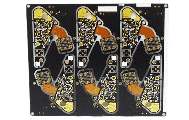
Huihe six-layer rigid-flex HDI original catalogue panel
Six-layer 2R + 2F + 2R construction, described for automotive radar.

Six-layer rigid-flex with one-step HDI

The catalogue gives 1.6 mm thickness and 4/4 mil trace/space, with 0.2 mm through-hole and 0.07 mm blind-hole notation. The latter is a specific example, smaller than the general rigid-flex table's 0.075 mm laser-hole field. Confirm the proposed drill and lamination route rather than assuming this exception is routine.

Supply the installed bend drawing, flexible-zone layer stack, bend radius and expected cycling. Agree coverlay, rigid-to-flex transition and coupon positions. The page identifies an automotive-radar application; it does not provide radar performance or bend-life results for the pictured board.

PROCESS WINDOWS / VOLUME, SAMPLE & SPECIFIC EXAMPLE

The same manufacturer publishes more than one production window.

Rigid volume work

1–20 layers; 500 × 600 mm maximum; 0.20–4.00 mm board thickness; 0.10 mm minimum trace and space; 10:1 aspect ratio; ±10% impedance tolerance.

Rigid samples

2–28 layers; 580 × 800 mm maximum; 0.20–6.00 mm board thickness; 0.075 mm minimum trace and space; 13:1 aspect ratio; ±10% impedance tolerance.

Rigid-flex table

Samples 2–32 layers; batches 2–20. Trace/space is 0.05 mm for samples and 0.075 mm for batches. The table separately lists routine ±10% and special ±3% impedance tolerances; the special tolerance needs a construction-specific agreement.

The rigid table explicitly distinguishes mechanical drill diameter 0.15–6.35 mm from mechanical finished-hole diameter 0.10–6.30 mm. The individual catalogue cards simply say “minimum hole”, so their holes remain unspecified as finished diameter in the RFQ. The homepage's ±5% statement describes impedance-line width tolerance, not ±5% electrical impedance.

Huihe ten-layer ENIG precision PCB original photograph
Ten-layer precision FR-4 catalogue example.

Ten-layer FR-4 example: inspect the layer-specific routing.

The catalogue specifies 1.0 mm thickness and ENIG; outer trace/space is 4.5/2.5 mil, inner is 4/3.5 mil, and the minimum-hole field is 0.3 mm. Its 2.5 mil outer spacing is narrower than the standard sample table's 0.075 mm, so request confirmation of the particular process and yield assumptions.

Attach the copper schedule, fine-spacing locations and agreed electrical test coverage. Do not combine this example's fine spacing with the table's maximum size, layer count or finished-hole limit.

PURCHASE RELEASE / SITE DOCUMENTS, TESTS & SCHEDULE

Ask for the dated documents that apply to the board you order.

Qualification scope at Building 2

The posted TÜV Saarland IATF copy names Xinfeng Huihe at Building 2, Xinda Park, and PCB manufacture excluding product design. It prints 0515729 / C300830 and 5 May 2024–4 May 2027. The hosted UL compliance certificate is dated November 2012, names E358408 and multilayer type hh02g4; it is not a current file-ownership or construction check.

The ZTW ISO 9001, 14001 and 45001 copies distinguish registration ending March 2028 from the current certificate validity ending 19 March 2026. The posted ISO 13485 copy ends 14 March 2025, and the posted pollution permit ends 27 June 2025. Obtain updated documents and their surveillance/issuer status rather than interpreting the longest printed date as current approval.

Product reports have narrower coverage

The CQC copy describes double-sided/multilayer FR-4, model 6160, 0.5–3.2 mm, V-0, with a printed period ending 4 March 2029. The July 2024 railway R24/R25 report front pages name an FR-4 PCB sample of 0.8–2.5 mm and HL3 findings; they are not blanket railway approval for RF or rigid-flex boards. RoHS, REACH, POPs and PFAS entries on the website are sample reports, not interchangeable factory management-system certificates. Request the complete applicable report, sample construction and test revision.

Testing and delivery inputs

The production page describes AOI, fixture and flying-probe open/short tests, dimensional inspection, X-ray registration checks and a physical/chemical laboratory. Its “functional problem” wording refers to bare-board continuity in the electrical-test descriptions; it does not establish assembled-device functional testing. Confirm coverage, fixtures, coupon measurement and the documents supplied with your lot.

The delivery table relates time to both layers and order area: a two-layer lot up to 1 m² is listed at 4 days, while the 100–300 m² column is 12 days; a ten-layer lot is 8 versus 16 days. Orders of 14 layers or more and over 300 m² require discussion. Rigid-flex sample times are separately listed, including six-layer work at 7 days expedited or 15 days normal. Confirm calendar, engineering-release start, laminate procurement and special-process additions.

The official contact page publishes em08@huihepcb.com and +86 181 7979 1130. That is a website-published contact, without a mailbox-control test or message sent during this review.

Prepare your stack & acceptance brief →
SOURCE TRAIL

Sources behind this profile

Individually researched 8 October 2026. Original product photos are paired with their adjacent construction specifications, not their changing article alt text. Manufacturer-hosted certificate and report copies were read; current issuer status and a factory audit were not established.

  1. ManufacturerLegal entity and manufacturing base ↗
  2. ManufacturerVolume, sample and rigid-flex process tables ↗
  3. ManufacturerCastellated examples and design guide ↗
  4. ManufacturerResin and electroplated via-in-pad examples ↗
  5. ManufacturerMixed-laminate and PTFE examples ↗
  6. ManufacturerHeavy-copper examples ↗
  7. ManufacturerRigid-flex constructions ↗
  8. ManufacturerPrecision multilayer catalogue ↗
  9. ManufacturerEquipment and electrical-test descriptions ↗
  10. ManufacturerOriginal qualification copies ↗
  11. ManufacturerLayer and area delivery tables ↗
  12. ManufacturerOfficial contact ↗
  13. GovernmentXinfeng September 2026 recruitment notice, entry13 ↗
Share with your sourcing team

Send the page to a colleague or save it in your project conversation.

LinkedInXFacebookWhatsAppTelegramRedditEmail