Start with the circuit's job, then define its construction.
Huizhou Hosond PCB Co., Ltd. · 惠州市和信达线路板有限公司 presents a Huizhou fabrication business at Jinji Industrial City, Xiaojinkou, Huicheng District, Guangdong. Its official English company page dates the operation to 18 December 2001 and describes a Hong Kong–China PCB manufacturing business focused on automotive electronics, with other industrial and communications applications.
The English catalogue is particularly useful: it publishes eight separate layer/line/space/drill constructions. The Chinese site supplies broader automotive, power, high-frequency, special-material and aluminium galleries. These two source sets are kept separate below; an attractive board photograph is not a substitute for its fabrication drawing.
For an initial shortlist, choose the automotive FR-4 or RF construction, compare the finish-specific multilayers, or start an aluminium thermal-material review. Each selection stays inside PCBVerified and carries only its own published values into the RFQ.
TWO ENTRY POINTS / AUTOMOTIVE FR-4 & RF MATERIAL
Two documented examples lead to different engineering reviews.
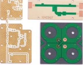
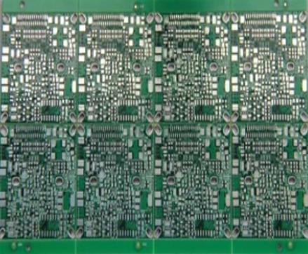
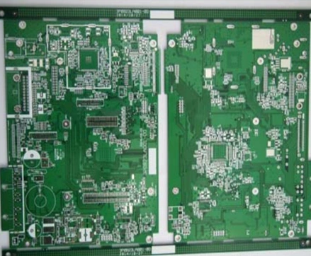
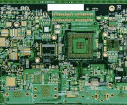
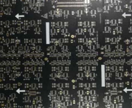
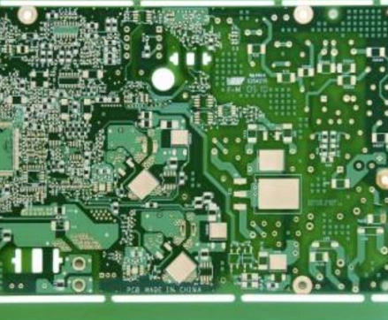
The four-layer automotive entry explicitly names FR-4 and ENIG. The two-layer high-frequency entry names OSP and a Teflon material, misspelled “Telfon” in the source. Its photographs show a catalogue group; they do not identify a specific laminate grade or measurable RF performance.
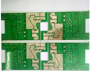
Original image beside this construction's English specification.
Four-layer automotive FR-4 / ENIG
Layers
4
Line / space
0.1 / 0.1 mm
Minimum drill diameter
0.2 mm; not a finished-hole limit
Material
FR-4
Surface finish
ENIG
Release the four-layer stack, finished copper, hole tolerances, finish thickness and programme-specific lot records. Automotive application wording does not approve a particular vehicle programme.
Original image beside this construction's English specification.
Two-layer high-frequency / OSP
Layers
2
Line / space
0.15 / 0.1 mm
Minimum drill diameter
0.4 mm; not a finished-hole limit
Material
Teflon, written “Telfon” on the source; grade unspecified
Surface finish
OSP
Confirm the exact PTFE laminate and bond system, copper, intended frequency, dielectric data and plated-hole process. Do not infer a Rogers grade or RF loss from these catalogue photographs.
Drill diameter and finished hole are different acceptance fields.
The eight English examples explicitly say minimum drill hole diameter. Plating and the finished-hole tolerance are not supplied. Their drill values remain visible here, while the directory's finished-hole field stays unknown. Release a finished-hole table, tolerances and plating allowance before relying on a hole-size filter.
The drilling-equipment page separately states 1–12 layers, a 0.2 mm minimum hole and 0.075/0.075 mm line/space. Those are undated general envelope claims; they do not replace the larger values attached to individual catalogue examples or establish a simultaneous combination.
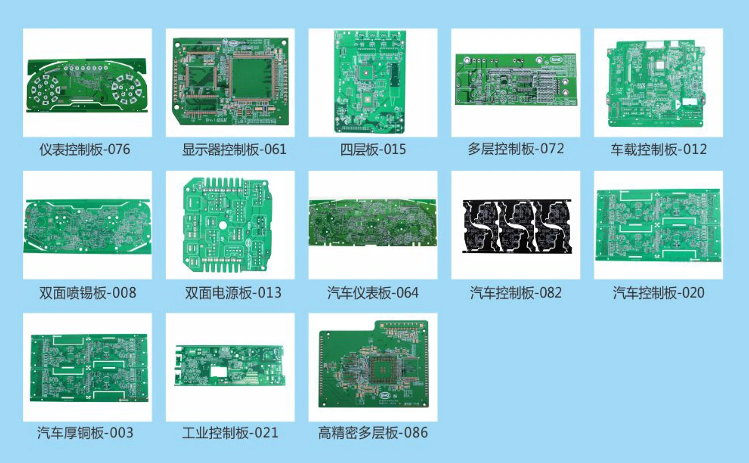
See the Chinese automotive catalogue and its board referencesThe original gallery names instrument-control 076, display-control 061, four-layer 015, multilayer-control 072, vehicle-control 012/082/020, double-sided HASL 008, double-sided power 013, automotive instrument 064, automotive heavy-copper 003, industrial control 021 and high-precision multilayer 086.
These are source reference labels, not assumed orderable stock models. No line/space, board thickness, copper weight or automotive qualification is attached to these Chinese photographs. The catalogue's heavy-copper label does not state an ounce value.
SIX SEPARATE CONSTRUCTIONS / FINISH & STACK
Specify what the finish must do in your assembly.
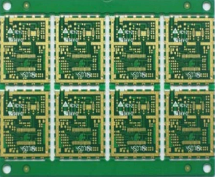
Hosond's remaining English examples separate immersion gold, lead-free HASL and gold plating. Preserve the chosen layer count and routing values, then complete the material, copper and thickness schedule. Their catalogue photographs are shown intact; the page does not publish a standard board thickness or an example-specific impedance tolerance.
Official English product catalogue · separate construction record.
Four-layer immersion-gold PCB
Layers
4
Line / space
0.101 / 0.101 mm
Minimum drill diameter
0.2 mm; not a finished-hole limit
Material
Not specified
Surface finish
Immersion gold
Provide the stack and pad-finish acceptance, including nickel/gold requirements where relevant. The source names immersion gold without a complete chemistry or thickness specification.
Official English product catalogue · separate construction record.
Six-layer lead-free HASL PCB
Layers
6
Line / space
0.1 / 0.1 mm
Minimum drill diameter
0.25 mm; not a finished-hole limit
Material
Not specified
Surface finish
Lead-free HASL
Agree the six-layer stack, solder alloy, finish flatness and assembly pad geometry. Assess HASL suitability against your component pitch and soldering plan.
Official English product catalogue · separate construction record.
Four-layer lead-free HASL PCB
Layers
4
Line / space
0.101 / 0.101 mm
Minimum drill diameter
0.30 mm; not a finished-hole limit
Material
Not specified
Surface finish
Lead-free HASL
Specify the board thickness, solder alloy and acceptance of finish coverage and planarity. Keep its 0.30 mm drill reference distinct from the four-layer ENIG example.
Official English product catalogue · separate construction record.
Six-layer gold-plated PCB
Layers
6
Line / space
0.1 / 0.13 mm
Minimum drill diameter
0.3 mm; not a finished-hole limit
Material
Not specified
Surface finish
Gold plating
Identify the plating zones, alloy, nickel underplate, thickness and contact duty. The term gold plating does not establish hard-gold composition, wear life or a gold-finger specification.
Official English product catalogue · separate construction record.
Two-layer immersion-gold PCB
Layers
2
Line / space
0.101 / 0.101 mm
Minimum drill diameter
0.30 mm; not a finished-hole limit
Material
Not specified
Surface finish
Immersion gold
Release the two-layer copper and pad geometry, finish requirements and test netlist. Do not substitute the separately pictured RF material or a multilayer stack.
Official English product catalogue · separate construction record.
Eight-layer immersion-gold PCB
Layers
8
Line / space
0.101 / 0.101 mm
Minimum drill diameter
0.30 mm; not a finished-hole limit
Material
Not specified
Surface finish
Immersion gold
Supply the complete eight-layer stack, signal reference planes, impedance targets and coupon if required. No example-specific impedance tolerance is published.
ALUMINIUM-BASE CIRCUITS / THERMAL & ISOLATION DATA
The thermal path starts with the dielectric specification.
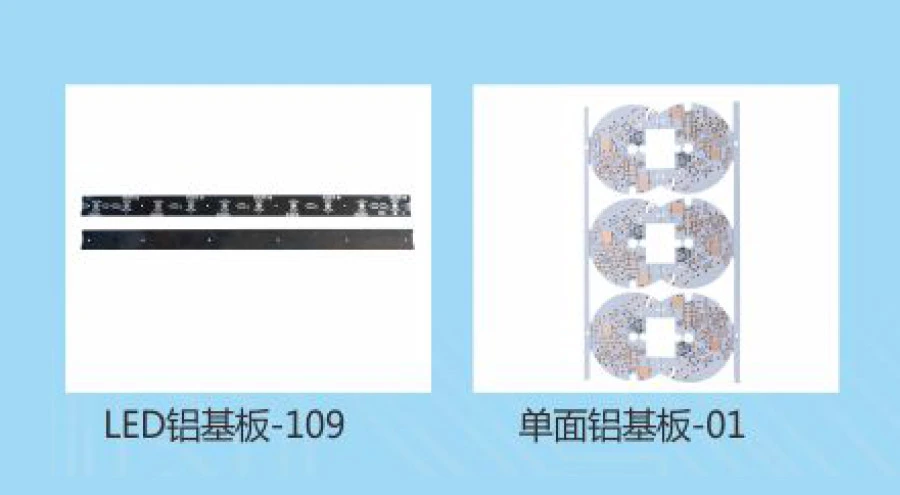
The Chinese aluminium catalogue labels LED aluminium-base board 109 and single-sided aluminium-base board 01. They establish a published product family, but do not state metal thickness, dielectric grade, thermal conductivity, isolation voltage or finished copper.
For an LED or power design, provide the heat load, operating conditions, mounting/thermal interface and circuit isolation requirements. Ask for a named base and dielectric construction with material documentation and the agreed test conditions. A metal base by itself does not define the insulating layer's performance.
Two source-labelled originals; 109 and 01 are catalogue references.
FABRICATION & TEST / DEFINE THE SHIPMENT EVIDENCE
Turn the published process route into an acceptance plan.
Hosond's English process diagram follows laminate cutting, inner layers, brown oxide and pressing, then drilling/PTH/plating, imaging and etching, solder mask and silkscreen. It also lists finishing, V-cut, routing/punching, electrical test, final inspection, packing and a Shenzhen warehouse step. This is a manufacturer process description; confirm the responsible site and any subcontracted steps for your order.
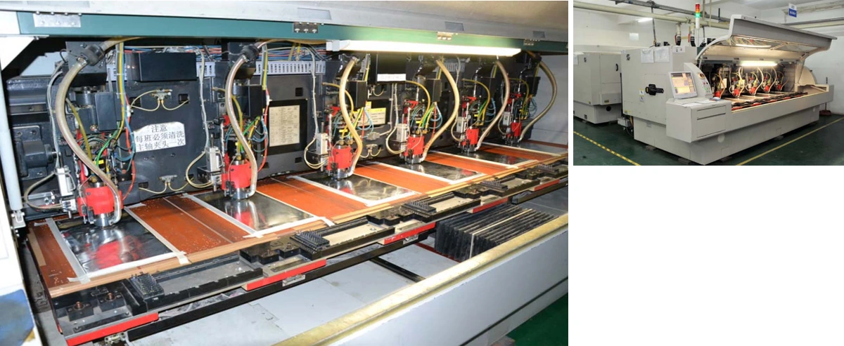
Official drilling-equipment page. The photo does not supply a calibrated capability or current utilisation record.
Drawing and tooling release
Agree drill/finished-hole definitions, stack revision, panel tooling, V-score or routed separation, edge clearance and measurement points. The organisation chart includes CAM, new-product sample management, planning, incoming/process/final inspection, electrical testing and physical laboratory responsibilities. Request the actual approval and escalation contacts rather than assuming the chart guarantees the current workflow.
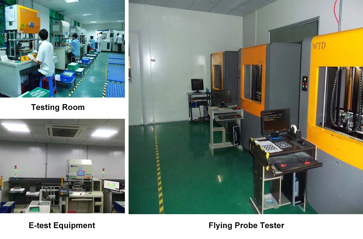
Test room, E-test equipment and flying-probe tester — labels retained from the original gallery.
Netlist and dimensional acceptance
Release the approved netlist, electrical-test coverage and report format, plus finished-hole and outline tolerances. Agree which checks apply to each shipment and how non-conforming lots are contained. A photograph of test equipment does not provide the actual lot's results.
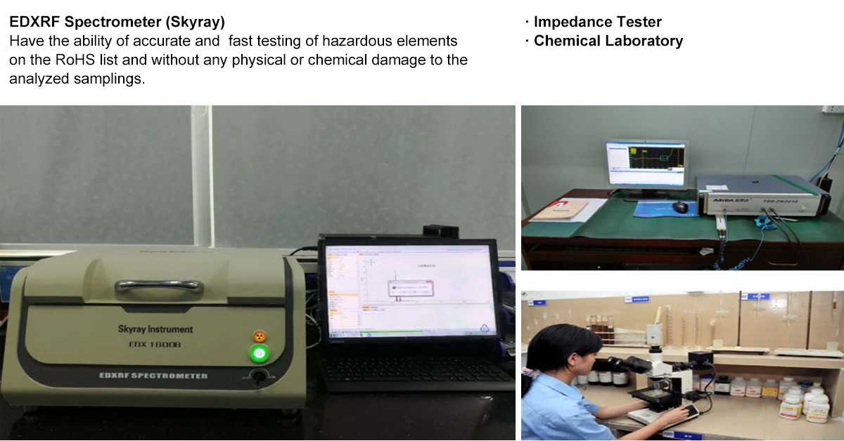
Reliability-inspection gallery: source-labelled Skyray EDXRF, impedance testing and chemical laboratory.
For controlled impedance, specify the target, tolerance, coupon, measurement method and reporting; the catalogue gives no construction-specific tolerance. For restricted-substance requirements, agree the material declaration, lot sampling and analytical evidence. The EDXRF gallery's screening description is not a blanket RoHS conformity result for every finished board.
QUOTE RELEASE / SITE, DOCUMENTS & PRODUCTION CLOCK
Make the first quotation specific enough to compare.
Choose the exact construction. Identify the catalogue reference, but release your own stack, material grade, copper, finished holes and drawing revision.
Define the finish and tests. Specify chemistry, thickness or alloy where relevant, assembly acceptance and shipment reports.
Identify who manufactures and ships. Match the legal entity and Xiaojinkou supplying site to the quotation; clarify the Shenzhen warehouse and any external process.
Obtain a live production schedule. Quantity, material availability, engineering approval date, working-day basis and delivery terms belong in the quotation.
The English introduction reports 10,000 m² floor area and 20,000 m² plant area, while Chinese text and home counters use a 10,000 m² workshop description. The undated 50,000 m²/month figure is a published capacity claim, not available capacity or a reserved production slot. Keep those measures and dates distinct.
The official contact pages publish market@pcbhxd.com.cn and mobile +86 13794095750. Reading the mailbox on the website does not verify its control. Enquiries can be prepared here without leaving PCBVerified.
Automotive and ISO documents need current, site-specific copies
The Chinese honours collage shows ISO 9001:2008, ISO 14001:2004 and ISO/TS 16949:2009 copies. Its page text also describes past audits and historical environmental/clean-production awards. These old versions are not shown as current certifications.
Obtain current issuer-register details, supplying-site address, certificate dates and scope for the programme. The official English history's customer references are manufacturer claims, not independent proof of present customer approval.
UL E256286: match the construction, not only the number
The manufacturer honours collage displays UL File E256286. Chinese text names HSD-DS double-sided, HSD-ML/HSD-ML-1 multilayer/heavy-copper and HSD-AL/HSD-AL-1 aluminium series.
This review did not establish the current holder and construction conditions from a live UL registry. For a UL-dependent order, obtain the applicable current record and match material, thickness, copper and temperature/flammability conditions to the actual board. No ownership badge is inferred from a historical collage.
SOURCE TRAIL
Sources behind this profile
Individually reviewed 9 October 2026: Chinese company and six catalogue collages, English image-adjacent construction records, history/process/equipment pages, original qualification images and the full government PDF. Parameters remain attached to their own examples; drill values are not finished holes. Historical papers and undated production figures do not establish current status or lot acceptance.