Optical-module PCB
Six layers, named Panasonic laminate and nickel–palladium–gold finish. Check bonding and pad metallurgy.
Compare the signal constructions →

MANUFACTURER DOSSIER
深圳市宏联电路有限公司 · Guangdong
Shenzhen Honlynn Circuit Co., Ltd. · 深圳市宏联电路有限公司 publishes multilayer, quick-turn and special-process PCB work from Shenzhen. Its contact page identifies Building 3, Floor 8, Jiangbi Environmental Technology Innovation Industrial Park, Jiangbian, Songgang, Bao'an. The Chinese name is the useful identifier for matching an order, site document or certificate; “Honglian” is the name used in this directory; the original photographs use the HONLIGHT CIRCUITS mark.
The company's introduction dates its establishment to March 2014 and describes 10,000-plus m² of workshop, with a reported 300,000 ft²/month capacity, including 50,000 ft² of small and medium batches. The homepage has a different 20,000 m² workshop statement. Confirm the production area and line assigned to your order; neither figure measures today's available delivery slots.
Six layers, named Panasonic laminate and nickel–palladium–gold finish. Check bonding and pad metallurgy.
Compare the signal constructions →Four-step and two-step examples with separate layer counts. Check via spans and the build-up drawing.
Review the two HDI examples →Different mechanical and conductor requirements. Resolve source-table differences before release.
Inspect the mechanical interfaces →A Shenzhen Industry and Information Technology Bureau subsidy list names the same Chinese legal entity in Bao'an, at entry 13191. This is a dated government identity record, not a fabrication audit or evidence that a particular machining limit has been achieved.
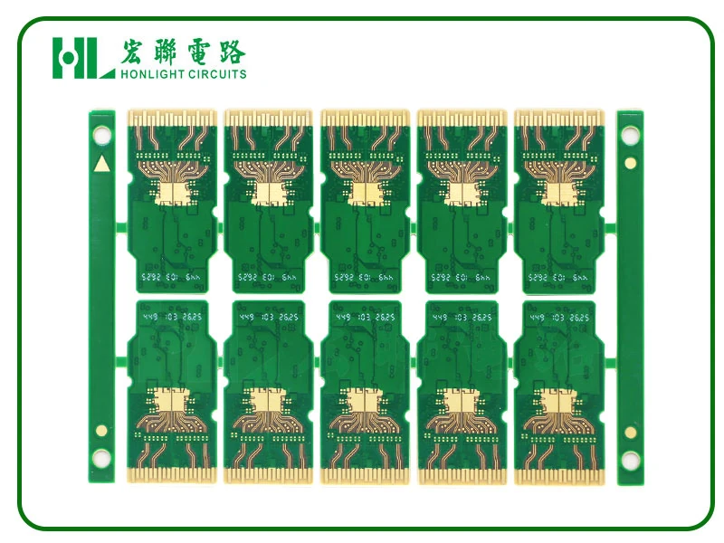
The product page pairs this board with resin-filled and capped holes and impedance control. It gives 0.5 oz outer copper; the inner-copper cell is printed “0.50Z”. Obtain the released copper schedule rather than interpreting the typography as a verified inner-layer weight.
Tell the factory whether the pads will be soldered, wire bonded or used for another contact interface. Agree nickel, palladium and gold thicknesses, surface preparation and the corresponding acceptance method. “Nickel–palladium–gold” alone does not establish a bonding qualification.
The page's parameter subheading says “six-layer one-step HDI”, while its main optical-module description does not define a microvia stack. Request the via cross-section and lamination drawing before classifying this example as an HDI route.
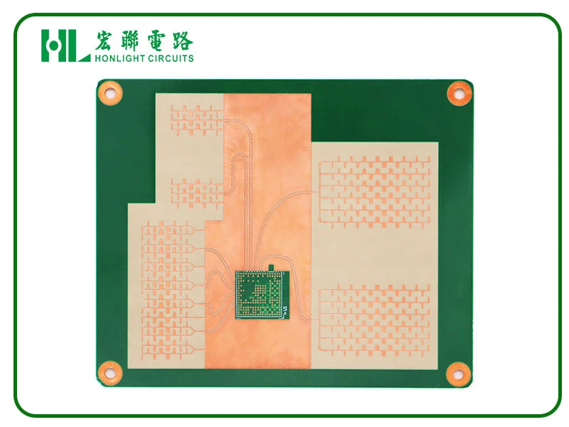
The original page describes resin filling, blind/buried vias and controlled impedance, with a 0.20 mm minimum-drill field. It supplies neither a Rogers grade nor a measured electrical-impedance tolerance. Its Dk 3.2 entry lacks a frequency, test method and layer allocation.
Release the exact Rogers part number, FR-4 grade, bondply and dielectric thickness of each signal layer. Define RF reference planes, the impedance coupon and any loss or phase measurements you expect. The optical example's tighter spacing and nickel–palladium–gold finish do not transfer to this OSP hybrid.
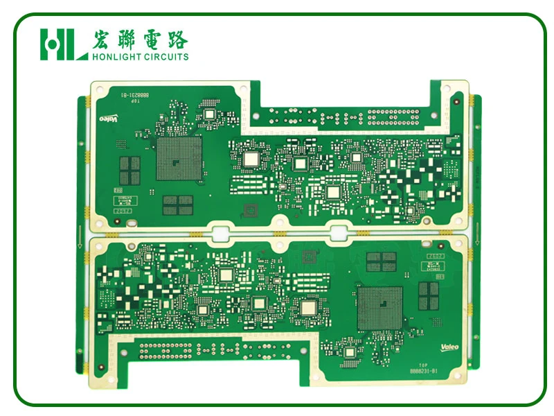
The named material is Shengyi S1000-2M, with 1.2 mm board thickness, immersion gold, 0.076/0.076 mm trace/space and 0.20 mm minimum-drill notation. The source associates it with industrial control, resin-filled holes and impedance control.
Ask which vias are stacked or staggered, which are filled and capped, and how the sequential laminations are arranged. A four-step label does not establish the via-span drawing or the microvia reliability test for your design.
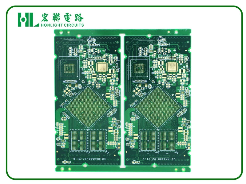
This separate S1000-2M example also lists 1.2 mm thickness, immersion gold, 0.076/0.076 mm trace/space and 0.20 mm minimum-drill notation. Its application cell says “POSS machine”; the exact equipment application should be clarified.
Compare it with the 12-layer board using the released via drawing and inspection requirements. More total layers do not mean more HDI build-up steps. Confirm the electrical-test access, filled-via inspection and any production-volume qualifications for the quoted stack.
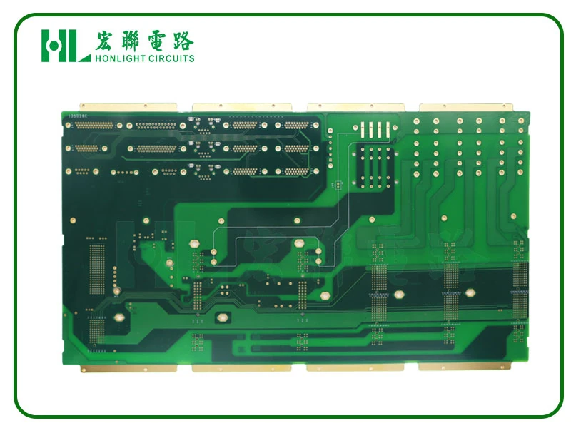
The table gives 2.5 mm thickness, immersion gold, 1 oz inner and outer copper, and 0.10/0.12 mm trace/space. The minimum-drill entry is 0.20 mm. Plugged vias and impedance control are named features.
The material description conflicts: the product summary specifies FR-4/TG170, while the detailed table says FR-4/tg150. The RFQ records FR-4 without choosing one Tg requirement. Specify the exact approved grade, Tg test method and thermal acceptance before quoting.
The source asks that plugged vias show no exposed red copper. Define the inspected surface, mask/plug acceptance and permitted depressions rather than inferring a fill type or thermal performance from the photograph.
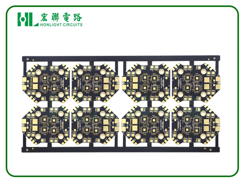
The detailed table names S1000-2M, 1.6 mm thickness and immersion gold, with a drone application. The summary gives 0.20 mm through holes and 0.075 mm blind holes.
The routing figures disagree: the summary says 75/95 µm trace/space, whereas the detailed table says 0.170/0.165 mm and lists 3 oz outer copper. Its inner field reads “30Z”. Routing values remain unset in the comparison/RFQ until the factory identifies the applicable copper and layer conditions.
Mark every plated edge and unplated break, the connection to internal planes, routing sequence and accepted edge coverage. Ask how the mechanical blind-via depth and conductor stack are controlled. A generic 0.075 mm hole cell is not a finished through-hole specification.
The process table lists 2–32 layers, 0.25–10.0 mm finished thickness, 17–420 µm finished copper and 0.075/0.065 mm minimum trace/space. The company introduction describes volume work through 24 layers. Ask which values are production-qualified for your size, copper and order quantity.
Do not combine the largest board, deepest stack, thickest copper and finest spacing into an assumed manufacturable design.
The maximum-size row pairs 1200 × 610 mm with “79 × 24 inches”; those are not equivalent dimensions. The 0.10 mm minimum-hole row is paired with 0.006 inches, also inconsistent. Request one released, unit-consistent drawing and specify whether holes are drilled or finished.
The catalogue's 0.075 mm blind-hole example is smaller than the general table's 0.10 mm blind/buried-via line. Treat it as a construction-specific question.
The workshop and inspection galleries separately identify LDI imaging, AOI, flying-probe testing, X-ray, impedance measurement, cross-section analysis and plating measurement. Ask which inspections and records apply to your lot, along with current calibration and coupon criteria.
The table describes 50–300 V bare-board open/short testing, a 245 ±5 °C three-second solderability test and a 288 ±5 °C, ten-second, three-cycle thermal-shock entry. Specify the applicable method, sampling and delivered results for the purchase order.
A row headed “ionic contamination” actually lists restricted substances at ppm levels. It does not provide an ionic-cleanliness measurement or its test method. Ask separately for cleanliness and material-compliance reports.
Supply the Gerbers, drill/via map, stack, approved laminate grades, copper schedule, outline and controlled finish zones. For the optical board include the bonding acceptance; for the RF hybrid include its electrical coupon; for the HDI boards include via-fill and sequential-lamination requirements; for metal edges include the edge-plating drawing.
The official contact publishes hlpcb@pcb-hl.com, 400 775 2975 and the market line +86 755 8172 0355. Ask which legal entity and production address will appear on the quotation, lot record and applicable certificates.
Prepare a construction-specific RFQ →The posted NQA IATF copy names PCB manufacture excluding design, T83500 / 0441195, and prints 16 January 2022–15 January 2025. Its Shajing premises differ from the current Jiangbi contact address. The posted ISO 9001 and 14001 copies, 04620Q10184R0S / 04620E10099R0S, end 30 March 2023 and also name the former premises.
The two UL compliance copies are dated 10 August 2015, with file E475833: HL-M multilayer and HL-D single-layer constructions. These hosted historical copies do not establish current file ownership or approval of the Jiangbi site. The CQC copies name HL-M / CQC17001180594 and HL-1 / CQC17001180846, each 0.38–6.0 mm, V-0, with former production addresses and continuing surveillance conditions. Obtain the current applicable issuer record and site schedule before specifying either mark.
Quick-turn service is advertised separately from the detailed board examples. Confirm when the delivery clock starts, which lamination cycles and materials are included, and whether quoted delivery is a ready-to-ship date or a received-by date.
Individually researched 8 October 2026. Each product uses its own manufacturer photograph and parameter page. Source-table differences are retained next to the affected construction. Government identity records do not certify PCB quality or process capability.
We use cookies to provide our services and measure website usage. Privacy policy