MANUFACTURER DOSSIER

Guilin Hengtai Electronic Technology

Official sources reviewed2026-10-09
GUILIN HENGTAI / PCB FABRICATION IN GUANGXI

A Lipu board manufacturer with a separate Shenzhen contact.

Guilin Hengtai Electronic Technology Co., Ltd. · 桂林恒泰电子科技有限公司 dates its establishment to 25 December 2018. Its manufacturing address is the Jinjiping high-technology industrial park in Lipu, Guangxi. The contact page identifies buildings 1, 15 and 18; the Shenzhen address is listed separately as a company contact, not as a second PCB fabrication site.

The original catalogue covers single-sided, double-sided, four-layer, multilayer and “high-precision” boards. The company introduction also names high-density and battery-specific circuit boards, with LED displays, communications and other application markets. Those application labels do not establish an automotive, medical or defence programme approval.

For buyers, the strongest starting point is a construction review of the five actual catalogue examples below. Only the single-, double- and four-layer titles specify layer counts. Material grades, hole dimensions and impedance requirements need to come from the released fabrication package.

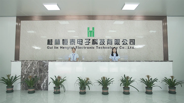
Guilin Hengtai official reception photograph with company name
The manufacturer's reception photograph. Guangxi Daily's 24 April 2025 report independently describes a visit to the same company at Jinjiping, Lipu.

Manufacturing location

Buildings 1, 15 and 18, Jinjiping High-Tech Industrial Park, Lipu, Guangxi.

Separate commercial contact

4th floor, Building 9, Nangang Third Industrial Area, Tangtou, Shiyan, Shenzhen. Agree which legal entity quotes, invoices and supplies the order.

CATALOGUE / CIRCUIT SIDES & PANEL DELIVERY

Single-sided and double-sided boards call for different release instructions.

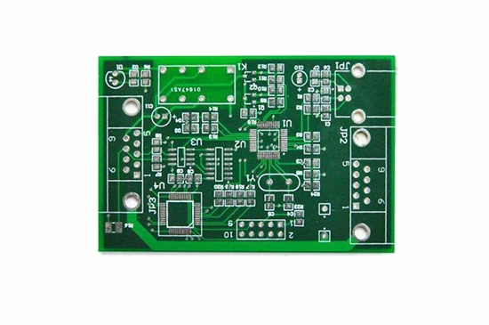
Hengtai original single-layer circuit board catalogue photograph
Official entry 6335897 · single-layer circuit board.

Single-layer circuit board

The title identifies one circuit layer. The original photograph includes component markings and mounting features, but the detail page supplies no substrate or finish specification. Do not infer paper phenolic, FR-4, copper weight or solderability from its appearance.

State the circuit side, component/legend side, laminate grade, outline, non-plated holes and any wire-link strategy. If copper is needed on both sides, use the separate double-sided construction rather than treating this single-layer entry as interchangeable.
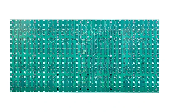
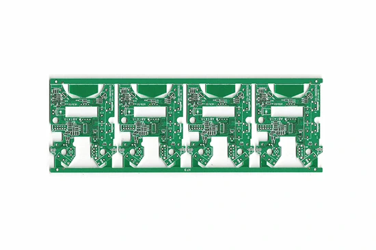
Hengtai actual double-layer board panel from its double-sided product detail page
Official entry 6351728 · double-layer circuit board.

Double-layer board: define the delivery panel

This is the actual photograph from the double-layer detail page, showing repeated board patterns on a panel. The panel dimensions, repeat count, break-off method and tooling arrangement are not product specifications in the source.

Supply a delivery-panel drawing with rails, fiducials, V-score or routing instructions and permitted scrap/X-out positions. For plated interconnections, define the finished hole and plating acceptance. Agree whether test is reported per delivered panel or per circuit and how a failed repeat is identified.

STACK-UP / FOUR LAYERS & A SEPARATE MULTILAYER ENTRY

Release the electrical stack and the mechanical interface together.

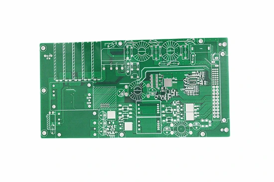
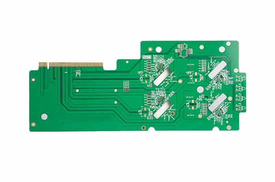
Hengtai four-layer circuit board original catalogue image
Official entry 6335997 · four-layer circuit board.

Four-layer board

The four-layer photograph shows an edge-contact area and a shaped outline. It does not specify a connector standard, contact plating system, bevel, mating-cycle life or dimensional tolerance. Put those requirements on the drawing if your assembly uses the edge interface.

Provide the four-layer assignment, dielectric thicknesses, copper weights and finished board thickness. If impedance control is needed, include net classes, target values, reference layers and coupon acceptance. A four-layer title alone does not promise a controlled-impedance construction.

Hengtai multilayer circuit board original image from its own multilayer detail
Official entry 6335917 · multilayer circuit board; exact layer count unpublished.

Multilayer board

The manufacturer's multilayer category and example are real, but this entry does not disclose its number of layers or via structure. It is not relabelled as a six-, eight- or HDI board.

Start the quotation with your proposed stack, drilled-hole table and expected production quantity. Ask engineering to confirm lamination sequence, registration, aspect ratio and cross-section acceptance for that construction. The high-density wording in the company introduction does not establish a blind-via or sequential-lamination process for this image.

HIGH-PRECISION CATALOGUE / REPEATABILITY BEFORE HEADLINE LIMITS

Translate “precision” into measurable acceptance.

Complete Hengtai high-precision board array original catalogue photograph
Official entry 6335922 · manufacturer's “high-precision” title. The source gives no numeric precision limits.

The image shows a repeated array with openings. It does not reveal the layer count, trace/space, minimum finished hole or laminate. Specify the features that matter to your assembly: hole-to-outline position, pad registration, routed opening geometry, solder-mask registration and finished thickness.

For LED-display or other repeated-board projects, agree the assembly fiducial system, panel flatness, test coverage and treatment of rejected circuits. These are procurement questions for your design, not a claim that the pictured array belongs to a particular customer's display module.

The site's “process capability” page is a photographic production gallery rather than a numerical process table. No image-derived measurements have been entered into this directory's numeric filters.

PRODUCTION / IMAGING, WET PROCESS & ELECTRICAL TEST

There are visible process resources. Tie them to the inspection plan.

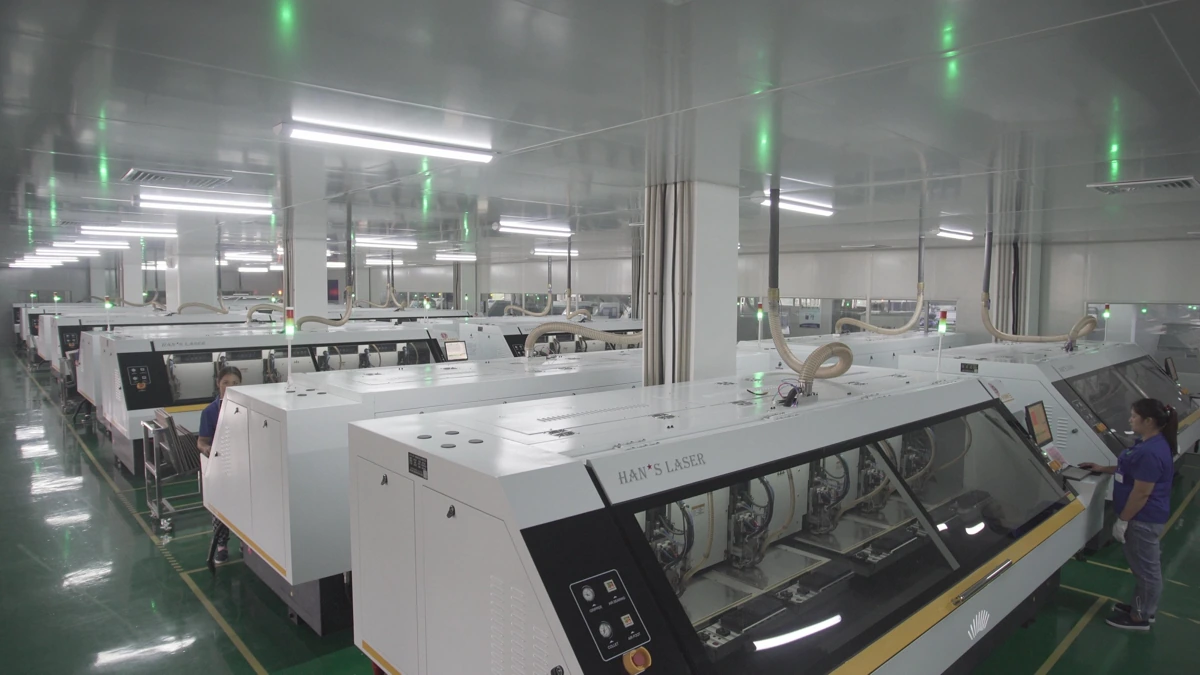
Hengtai official production photograph of circuit board drilling area
Original photograph from the manufacturer's process gallery. Equipment photographs do not establish calibration, utilization or the construction limits of an order.

Imaging and registration

The company and equipment pages name Weiying LDI, Keshi double-sided CCD, automatic film lamination, scanning equipment and an AOI repair station. Ask how inner-layer registration and optical inspection are controlled for the released stack, including defect repair acceptance.

Drilling and surface treatment

The gallery identifies Han's drilling equipment, automated copper-plating resources and an OSP anti-oxidation line. The company introduction separately mentions copper deposition, pattern plating and HASL. Choose a finish and hole construction explicitly; this equipment list does not assign OSP or HASL to every catalogue board.

Electrical and laboratory acceptance

The second equipment page names WTD high-speed flying-probe testing, a metallographic microscope, FQC and a laboratory. Agree netlist coverage, test settings, cross-section locations and delivered records. Bare-board continuity testing does not replace component-level functional or assembled-product testing.

Read the published scale and environmental context

The undated company introduction reports 20,800 m² of plant area, three factories, annual capacity of 3.2 million m² and monthly capacity of 260,000 m². These are manufacturer-reported scale figures, not a current capacity reservation. The dated Guangxi Daily report describes three workshops and six automated lines during an April 2025 visit; its date and narrower scope are retained.

The environmental page describes segregated collection and transfer to an industrial-park wastewater station rated at 15,000 m³/day. That figure belongs to the park treatment facility, not to a Hengtai-owned treatment line or a permitted discharge volume for your order. Request applicable current site permits if environmental documentation is part of supplier qualification.

PURCHASING / A CONTROLLED ORDER FOR THE LIPU SITE

Ask for a fabrication response that closes the open design decisions.

Send with the initial RFQ

  1. Board definition: copper data, netlist, layer assignment, approved laminate grade and thickness, finish and order quantity.
  2. Panel and interface drawing: rails, fiducials, break-off method, mounting/connector details, tolerances and X-out policy.
  3. Acceptance: applicable workmanship class, finished holes, copper records, electrical test, cross-sections and any impedance coupons.
  4. Commercial release: supplying entity, manufacturing location, engineering-query closure, agreed schedule, packing and delivery destination.

The official contact page publishes Hengtai@glhtpcb.com for Guilin and Market@glhtpcb.com for the Shenzhen contact. The source establishes publication of those addresses, not mailbox ownership verification. Keep your shortlist and fabrication request on PCBVerified.

Prepare a Hengtai fabrication brief →

Match qualifications to the supplying site

The qualification page displays ISO, IATF, CQC and UL graphics, with the labels UL E243002 and CQC12001085831. These are published claims rather than readable, current certificates. Its introduction says some systems are being applied for, while the company introduction describes operation to those standards. Obtain current issuer records, scope and site address before using an approval in a purchasing specification.

Patent copies are a different kind of document

The gallery includes five patent certificate fronts naming 桂林恒泰电子科技有限公司 and its Lipu park address. Three utility-model copies concern a heat-dissipating multilayer board, a printed-board structure and storage of an ultra-thin board, with August 2021 grant dates. Two invention copies show ZL201910277970.9 and ZL202010442398.X, both granted on 10 August 2021.

Each photographed copy is marked page 1 of 2. They identify historical patent documents; they do not establish current legal status, a commercially supplied model, a corrosion test result or a particular catalogue board's performance.

Independent site context

Guangxi's 18 April 2023 official report names the company among Lipu enterprises. Guangxi Daily's 24 April 2025 issue describes a visit to its Jinjiping production site. These dated records corroborate local company activity; they are not product certification or a factory quality audit.

SOURCE TRAIL

Sources behind this profile

Individually researched 9 October 2026. Five product detail pages and their complete original photographs were reviewed separately from the process, equipment, qualification, environmental and contact pages. The complete newspaper page and original official report were read. Product fields contain only explicitly named layer counts; the catalogue entry numbers are website identifiers, not manufacturer model numbers.

  1. ManufacturerCompany, establishment date and published production scope ↗
  2. ManufacturerLipu factory and separate Shenzhen contact ↗
  3. ManufacturerSingle-layer board, original entry 6335897 ↗
  4. ManufacturerDouble-layer board, original entry 6351728 ↗
  5. ManufacturerFour-layer board, original entry 6335997 ↗
  6. ManufacturerMultilayer board, original entry 6335917 ↗
  7. ManufacturerHigh-precision board, original entry 6335922 ↗
  8. ManufacturerProcess photographs and equipment gallery ↗
  9. ManufacturerEquipment gallery, including second page of test resources ↗
  10. ManufacturerQualification graphics and five patent certificate fronts ↗
  11. ManufacturerPark wastewater collection description ↗
  12. GovernmentGuangxi official report naming the Lipu company, 18 April 2023 ↗
  13. Original publicationGuangxi Daily, 24 April 2025, page 12; dated production-site visit ↗
Share with your sourcing team

Send the page to a colleague or save it in your project conversation.

LinkedInXFacebookWhatsAppTelegramRedditEmail