Guangdong headquarters
The issuer describes a focus on high-end optical-module and high-speed connector PCB development, with higher layers/build-up and AI-related work. Confirm the stack and bonding or connector interface with this division.


MANUFACTURER DOSSIER
广东科翔电子科技股份有限公司 · Huizhou, Guangdong, China
Checked on 29 October 2026 against the 2025 annual report on CNInfo, Shenzhen Stock Exchange listing data, the official website and UL iQ for Printed Wiring Boards. Ask which subsidiary will build your board; capabilities differ by plant.
Guangdong Kingshine Electronic Technology Co., Ltd. (广东科翔电子科技股份有限公司, stock code 300903) has its headquarters at 9 Longshan Eighth Road, Daya Bay West District, Huizhou. Its official company page dates its founding to 2001 and lists separate business divisions. The 2025 issuer report confirms the legal name and headquarters address, then describes a differentiated factory strategy for 2026. The practical purchasing question is which division accepts your construction and owns its release evidence.
The issuer describes a focus on high-end optical-module and high-speed connector PCB development, with higher layers/build-up and AI-related work. Confirm the stack and bonding or connector interface with this division.
The report positions Tean for mid/high-end communication and server PCBs; Jiangxi for high-order HDI, AI-server and automotive ADAS volume work. The quotation should name one producing entity and process route.
Ganzhou’s focus is power and energy boards; Shangrao is described around automotive power-protection and rigid-flex, while Guangzhou Taojidian focuses on ceramic substrates. These roles are not a single Huizhou process envelope.
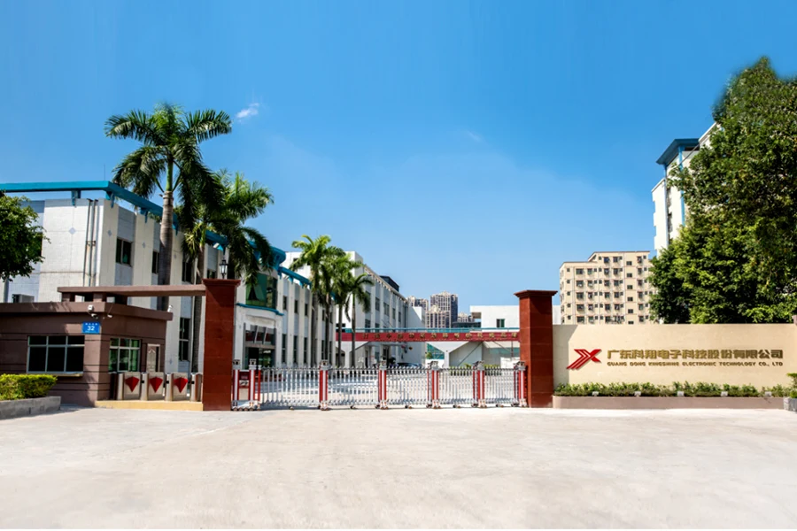
The group company page says seven divisions, while newer Chinese homepage development entries include mSAP/AI preparations. Counts and future projects do not establish current availability for a buyer. The original headquarters-division photograph below identifies a location; no equipment or layer capability is inferred from the exterior.
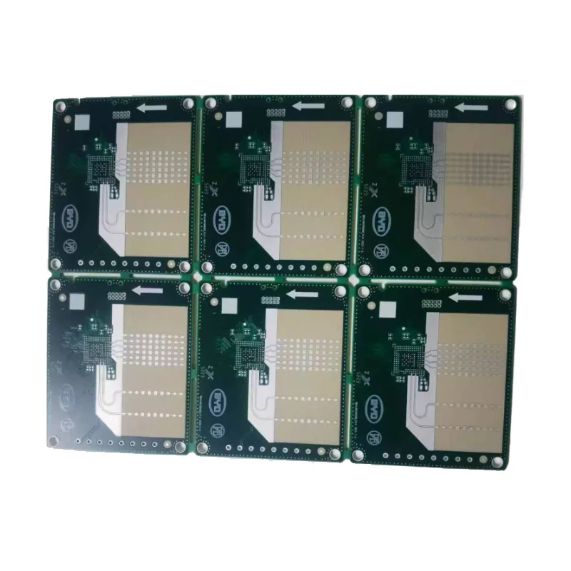
The source uses separate through-hole and blind-hole rows within one example. It does not explicitly define the minimum-hole values as drilled or finished dimensions. Put both definitions in your hole table and obtain the fabricator’s accepted values. Likewise, “high/low copper” is a construction note without numeric copper weights; it needs a layer-by-layer copper specification.
Assign the two materials to the actual stack layers and define the RF reference planes, dielectric thickness and required frequency/test band. For a mixed press, request the accepted lamination sequence and the relevant registration and section criteria. The gallery label “millimeter wave” does not supply a measured loss curve, operating band or antenna-performance result.
The line width and spacing are intentionally different: the original table states 267/96 μm, not 96/96. It calls out through-hole POFV without publishing a hole-fill or cap-thickness criterion. Specify the actual via locations, fill/planarity requirements and the finished-hole definition rather than using the catalogue hole value as a complete fabrication note.
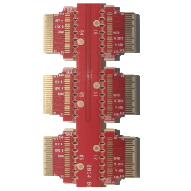
Separate the hard-gold contact areas from immersion-gold assembly areas in the drawing. Agree deposit thickness, contact geometry and the insertion-life qualification required by your connector. The table does not state a transmission rate, impedance target or wear-test result; those belong in the project specification.
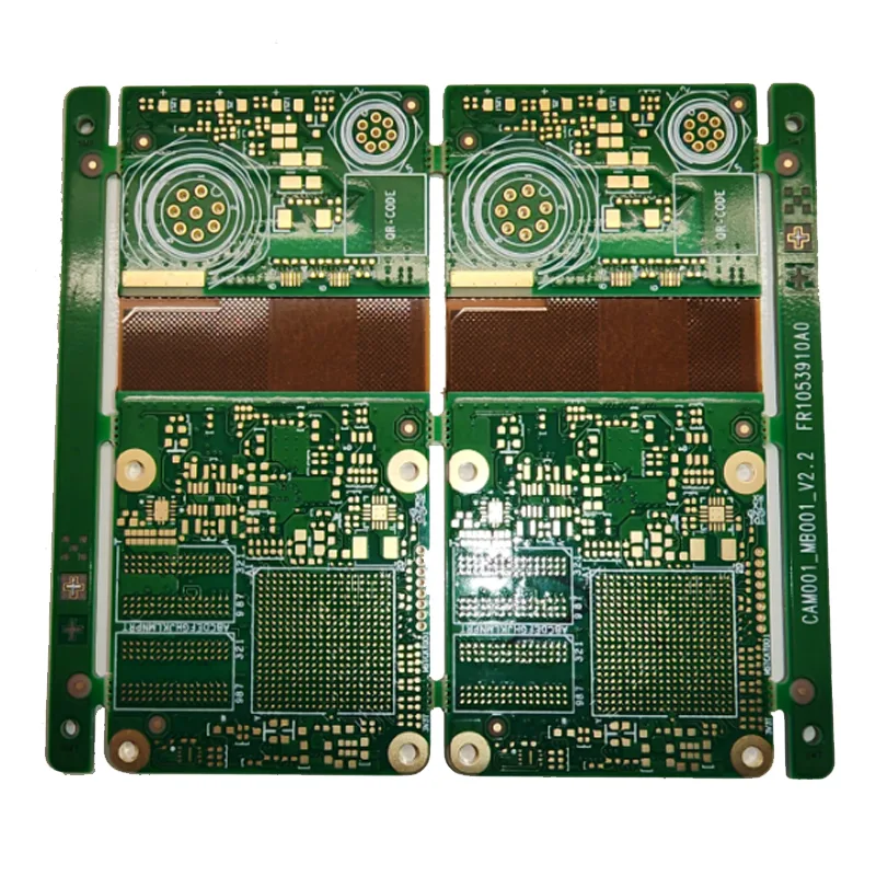
The original table names an opening in the rigid-flex region. Its material field does not supply a laminate grade or expand “CVL”; keep that shorthand in the review and request the full rigid/flex material list. No flexible-layer count, bend radius or dynamic bend life is established by this photograph.
Send a region drawing with the opening boundary, flex-to-rigid transition, layer termination and installed geometry. Identify RF routes and reference-plane continuity through the transition, and specify the intended movement and environmental exposure. Have the fabricator propose the region-specific stack, material and inspection plan before quoting this as a repeatable build.
The current manufacturer product center explicitly labels a Mitsubishi laser drill, an LDI machine, vacuum resin plugging, hole filling and a vacuum etching line. Its test-equipment entries include an impedance tester, network analyzer, blind-hole inspection machine, fluorescence-spectrum analyzer and ion-contamination tester. These are group gallery disclosures; model, quantity, calibration and division assignment are not supplied.
Request material-lot identity, accepted dielectric/copper stack, impedance coupons and a project-specific RF measurement scope. A pictured network analyzer does not define fixtures, test frequency, de-embedding or the loss limits included in the quote.
Request contact-finish measurements and the agreed hole-fill/cap sections. Link those results to the POFV locations and drawing revision. An equipment list cannot replace board-level acceptance.
Name the legal entity and division in the response, with sample-to-volume transfer requirements, approved material substitutions and lot/process change control. Request the actual lot report from that route.
The 2025 report’s project table describes blind-hole stack alignment and back-drill alignment projects as completed, with ≤15 μm and ≤25 μm respectively. Those are project disclosures, not the minimum hole size or residual-stub limit of the three boards shown above. The same report labels high-frequency microwave research and certain precision-routing work as research-stage activity. Do not turn those targets into a generic production guarantee.
The report separately presents a 400G/800G development row with 100 Ω ±5% differential impedance and a frequency-specific insertion-loss figure. It does not bind that row to this photographed six-layer optical board. Obtain the current coupon and test plan for your own construction. Material grades and loss requirements should remain in the same revision-controlled response.
Attach the selected construction, layer/region stack, copper and material definitions, finished-hole table and quantities. Add radar frequency/loss requirements, optical contact finishes, or rigid-flex movement geometry as appropriate. Ask for accepted exceptions, the named production division, required qualification work and the release reports together.
The official contact page lists marketing@kxkjpcb.com for headquarters and several divisions, with a separate Ganzhou contact. The issuer’s investor mailbox serves securities matters. A published address is retained as source information, not proof of delivery or a reason to send a test marketing message.
Prepare the fabrication brief → · Compare RF constructions →Individually researched on 8 October 2026. The three specification tables are images on their corresponding official detail pages and were read visually. Product examples, group equipment, dated R&D and future division strategy retain their distinct scopes.
We use cookies to provide our services and measure website usage. Privacy policy