GUANGDE TONGLING / CHOOSE THE PHYSICAL BOARD FIRST
A long lighting strip, a thermal base and a contact board need different briefs.
广德通灵电子有限公司 / Guangde Tongling Electronics publishes a particularly useful mix of long lighting boards, small outlines, thermally conductive CEM-3 and aluminum-base examples, plus single-sided, double-sided and multilayer boards with distinct finishes. Start with the mechanical envelope and heat path, then release the stack and surface requirement.
The Guangde company dates its establishment to 2014 and production to 2016. Its earlier Wujiang business history is discussed separately below. Ten selected references retain the exact corresponding catalogue images; a general factory limit is not assigned to a photographed sample.
MECHANICAL ENVELOPE / LENGTH DOES NOT DEFINE A PANEL
Resolve finished length, support and separation before pricing.
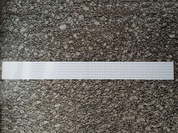
One-metre board — catalogue reference
Catalogue title
One-metre board
Actual dimensions / layers
No dimensional drawing or stack published
Provide a dimensioned outline, panel and breakaway design, mounting pitch, bow/twist acceptance and handling constraints. The title does not define finished length tolerance or the usable manufacturing panel.
Long-board release
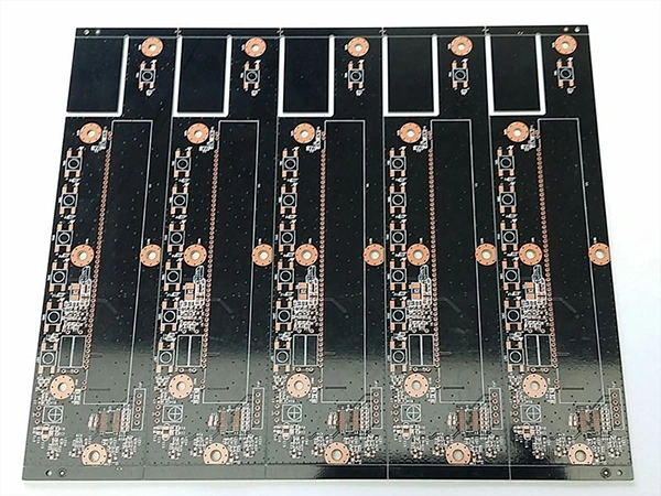
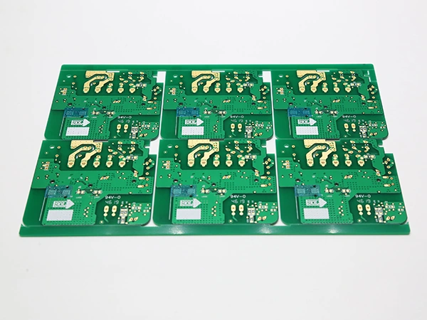
The catalogue has three distinct entries: a one-metre board, a one-metre lighting board and a long lighting board. They supply family labels and photographs, not dimensioned drawings. Define usable length and width, mounting datums, permitted bow/twist, breakaway features and packaging. Confirm how the supplier will fixture, process and inspect your finished outline.
Special panel versus delivered part
The general process sheet lists 660 × 660 mm, with a special 1250 × 660 mm size. This is a published manufacturing envelope, not proof that every layer/material/finish combination can use the larger size. A long finished part and a manufacturing panel are separate dimensional requirements.
Small-format PCB — catalogue reference
Family
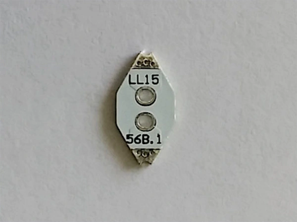
Small-format board
Published dimensions
Not supplied
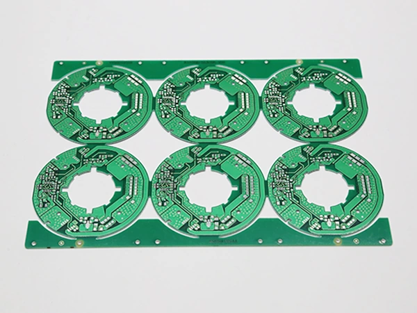
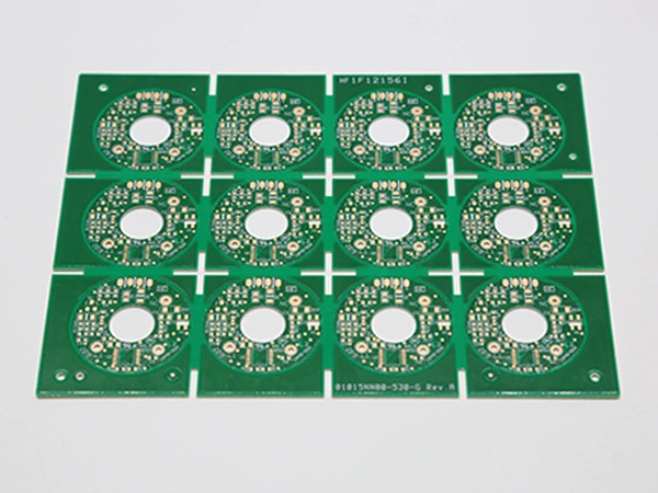
Specify component and hole registration, router or punch allowances, panel tabs and how the small board will be measured and electrically tested. Do not infer its dimensions from the printed markings.
For the small-format reference, the official page gives no dimensions. The photograph’s printed markings are not a dimensional specification. Agree measurement datums, panel tabs, registration and test access rather than estimating size from the image.
THERMAL PATH / TWO DIFFERENT SUBSTRATE FAMILIES
CEM-3 and aluminum base are separate sourcing choices.
Thermally conductive CEM-3 PCB
Published substrate
CEM-3
Thermal conductivity / dielectric
Not numerically specified
Request the exact laminate grade, thermal test conditions, dielectric isolation, copper and thickness. CEM-3 thermal-board wording does not make this an aluminum-base construction.
Aluminum-base LED board — catalogue reference
Published family
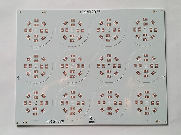
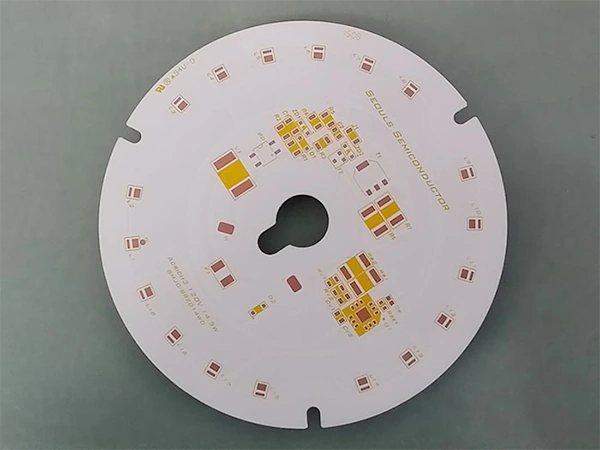
Aluminum-base PCB
Photograph
Board with mounted components
Stack / thermal rating
Not supplied
Define the base metal, insulating layer, copper and mounting heat path. Clarify bare-board versus assembly supply, electrical isolation and thermal acceptance; mounted LEDs in a photograph do not establish an assembly-service contract.
Ask for the dielectric, not just “good heat dissipation”.
The CEM-3 entry identifies its laminate family. It does not give a thermal-conductivity value, insulation rating, grade or delivered copper. The aluminum-base photograph includes mounted components, while its catalogue title identifies a board family. Neither establishes assembly supply, a dielectric breakdown result or the order’s thermal stack.
Release the substrate and insulating layer, copper, finished thickness, thermal interface, mounting details and acceptance conditions. Keep the bare-board and assembled-board deliverables separate on the quotation.
STACK / SOLDERABLE AREAS / CONTACT AREAS
A finish name is only the beginning of the specification.
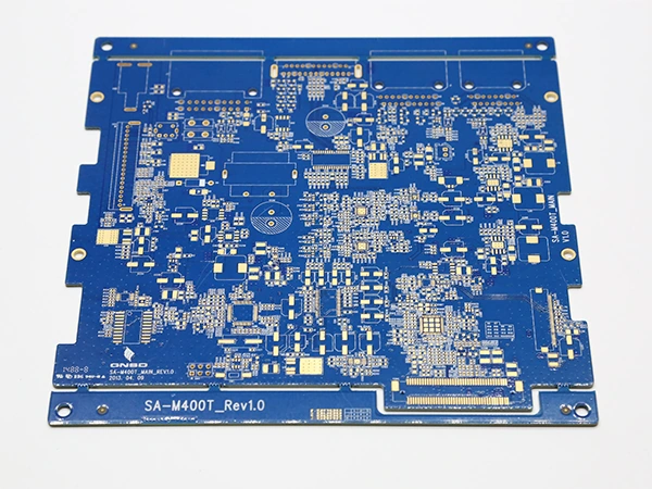
Six-layer immersion-gold PCB
Layers
6 — catalogue title
Finish
Immersion gold
Laminate / gold thickness
Not disclosed
Release the six-layer stack, controlled impedance and finish specification, including nickel/gold thickness and solderability requirements. The process sheet’s ±10% impedance limit is not this example’s test result.
Four-layer OSP PCB
Layers
4 — catalogue title
Finish
OSP
Copper / laminate
Not disclosed
Specify OSP chemistry or agreed acceptance, storage, handling and the intended assembly thermal cycles. Obtain the actual four-layer stack and electrical test plan.
The six-layer and four-layer counts are stated in the individual catalogue titles. Their laminate, copper and impedance construction are not published. The catalogue also contains four-layer HASL, double-sided OSP, electroplated-gold, immersion-gold and HASL examples. These are distinct references, not interchangeable finishes for a single board.
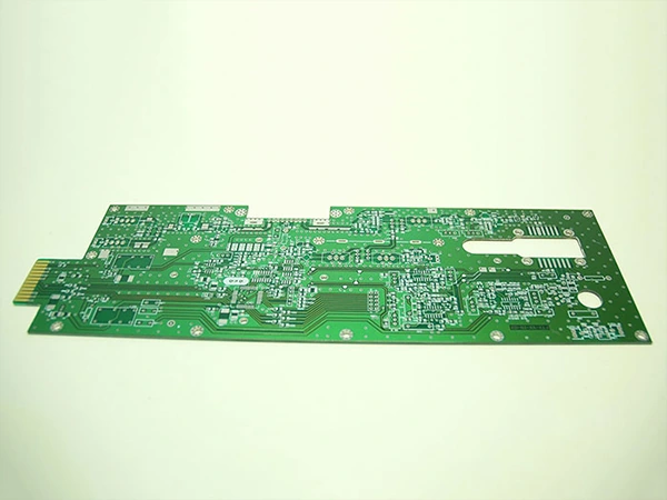
Double-sided gold-finger PCB
Construction
Double-sided
Contact feature
Gold fingers
Gold thickness / hardness
Not supplied
Define selective plating, contact finish thickness and hardness, bevel and dimensional datum, mating requirements and solderable areas separately. Gold-finger wording is not an immersion-gold specification.
Die-punched single-sided PCB
Construction
Single-sided — source category
Outline method
Die punching
Laminate / tolerance
Not supplied
Agree material, tooling ownership, burr limits, hole-to-outline registration and panel separation. The general routed-outline tolerance must not be assumed for the die-punched part.
Single-sided peelable-mask PCB
Construction
Single-sided — source category
Mask feature
Peelable mask
Material / protected regions
Drawing required
Mark protected pads and holes, mask compatibility, cure and removal requirements. Treat temporary peelable mask separately from permanent solder mask and the underlying surface finish.
Single-sided CEM-1 PCB
Construction
Single-sided
Laminate family
CEM-1
Source date
29 March 2017
Request a current CEM-1 grade, copper, insulation requirements and outline process. This older catalogue entry establishes a family reference, not current stock or a multilayer construction.
Contact surfaces, solderable surfaces and temporary masking need separate instructions. Specify selective plating and mating requirements for fingers; protected regions and removal for peelable mask; material and tooling for punched outlines. The older single-sided CEM-1 entry is dated 29 March 2017, so ask for the current grade and procurement conditions rather than assuming inventory.
PUBLISHED PROCESS SHEET / KEEP CONDITIONS ATTACHED
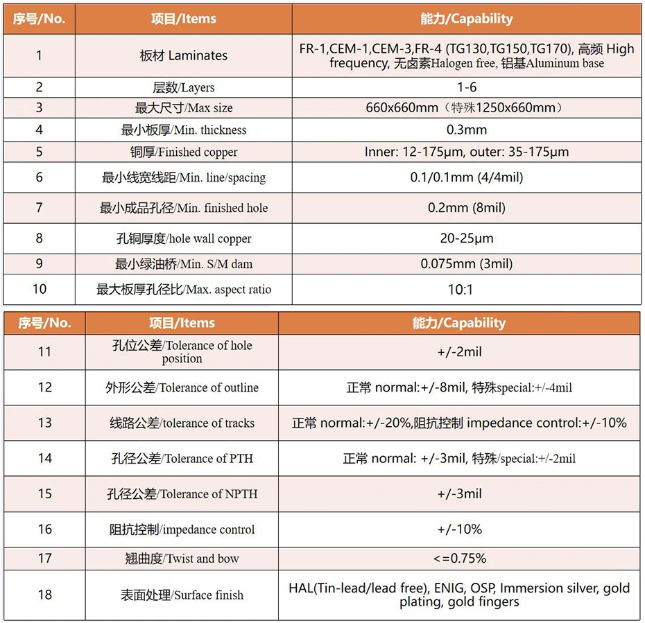
Use the 1–6-layer envelope for drawing review, not as a combined sample guarantee.
Construction and routing
Layers
1–6
Working size
660 × 660 mm; special 1250 × 660 mm
Minimum board thickness
0.3 mm
Finished copper
Inner 12–175 µm; outer 35–175 µm
Minimum line / space
0.10 / 0.10 mm
Holes and acceptance
Minimum finished hole
0.20 mm — explicitly finished
Hole-wall copper
20–25 µm
Maximum aspect ratio
10:1
Impedance control
±10% — general process value
Bow / twist
≤0.75% — confirm panel versus individual part
The sheet distinguishes hole-position tolerance (±2 mil), PTH diameter (normal ±3 mil / special ±2 mil) and NPTH diameter (±3 mil). It lists normal outline tolerance ±8 mil and special ±4 mil. Do not interchange these definitions or apply a routed tolerance automatically to a die-punched outline.
FR-1, CEM-1, CEM-3, FR-4 with TG130/TG150/TG170, high-frequency, halogen-free and aluminum-base families appear in the general material list. The individual example’s laminate grade and lot traceability still need a controlled bill of materials. Its finish list separates leaded/lead-free HASL, ENIG, OSP, immersion silver and plated contacts.
Read the original process-sheet imageOriginal Tongling process envelope; individual limits are not assigned to every catalogue board.
GUANGDE SITE / A PROCESS ROUTE TO CONFIRM
Identify the plant and ask how the construction moves through it.
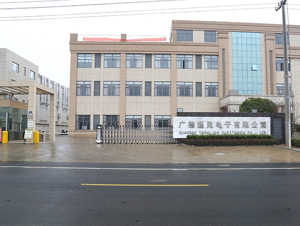
Original manufacturer photograph of the Guangde premises.
Separate the predecessor timeline
The official history starts with the Wujiang circuit-board accessories factory in 1978 and a Wujiang company in 2002. The Guangde entity was established in 2014; its company introduction says production began in 2016, and its history records second-phase investment in 2020 and equipment introduction/production in 2021. These dates describe different stages and entities.
The current published contact is No. 751 Chang’an Road, PCB Industrial Park, Guangde Economic Development Zone, Anhui. The official email is wy@tlpcb.com, telephone 0563-6988838. Reading an address is not a mailbox-control test; the quotation should name the actual contracting and producing entity.
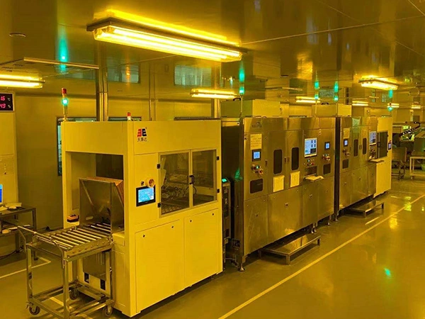
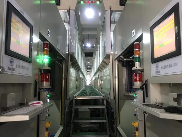
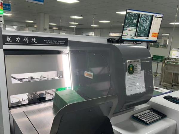
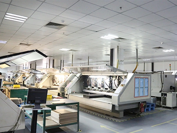
Official equipment entry: LDI exposure.Official equipment entry: VCP plating line.Official equipment entry: AVI appearance scanning.Official equipment entry: drilling workshop.
The individually read gallery also labels CCD exposure, AOI, PTH, OSP, etching, material storage, the laboratory and finished inspection. No model inventory, installed counts or available production capacity is inferred from these photographs. Confirm electrical test coverage, cross-sections and dimensional inspection against the actual construction.
The “capacity” page is a sales chart.
The reviewed image shows annual revenue for 2013–2024. It does not state available monthly board output or lead time, and part of that period precedes the Guangde company’s establishment. Request the current order schedule and site allocation rather than converting revenue into production capacity.
RECORDS / HOLDER, DATE AND CONSTRUCTION
UL ownership is readable; each delivered construction still needs its scope.
UL’s original holder record
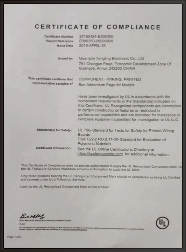
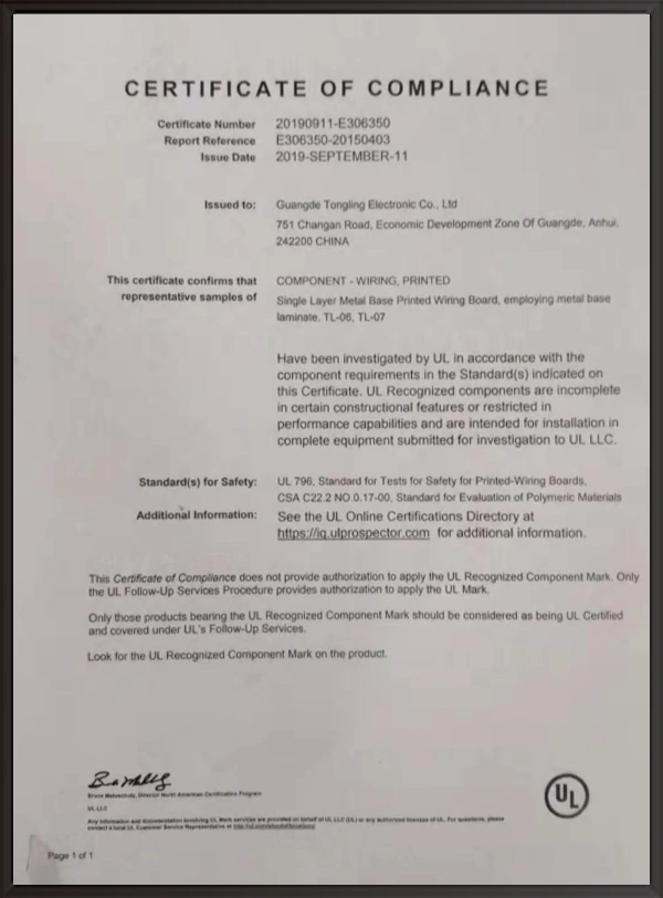
The UL Product iQ record ZPMV2.E306350, read 9 October 2026, names Guangde Tongling Electronic Co., Ltd as the holder for printed-wiring components and lists specific model designations. This establishes the published file-to-holder relationship; it does not map these ten catalogue photographs to the listed constructions.
The manufacturer’s 24 April 2019 copy is page 1 of 2 and refers to an addendum that is not shown. Its 11 September 2019 copy concerns single-layer metal-base models TL-06 and TL-07. Ask for the applicable current construction and mark/follow-up-service conditions for your order.
Original local public record
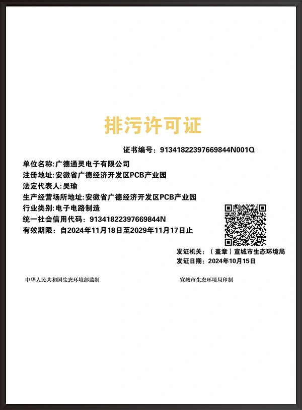
Guangde’s 2025 second-quarter permit table, row 85, records the exact Chinese entity, PCB park, electronic-circuit manufacturing and permit 91341822397669844N001Q, dated 18 November 2024–17 November 2029. It agrees with the manufacturer’s permit copy and supports the entity/site record. It does not establish PCB quality, equipment performance or compliance with a buyer’s individual programme.
PCB quality and automotive copies
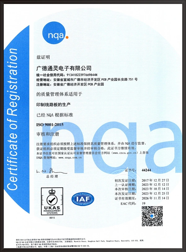
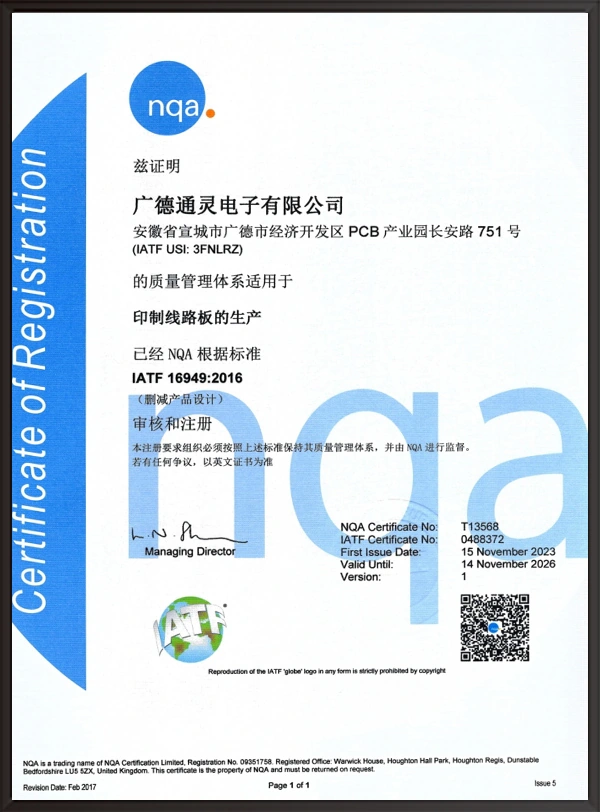
NQA ISO9001 certificate 44244 and automotive certificate T13568 / IATF 0488372 show validity to 14 November 2026. The automotive copy covers PCB manufacture and excludes product design. They are supplier-published copies; no current issuer-status badge is assigned from a printed expiry date.
NQA ISO9001 copyNQA ISO9001 copy — original supplier-published document.NQA IATF copyNQA IATF copy — original supplier-published document.
Environmental and substance-process documents
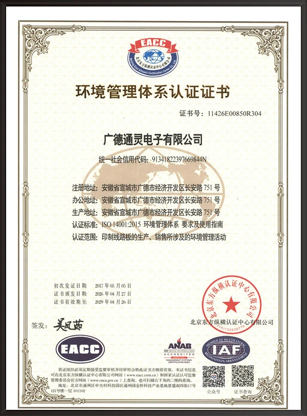
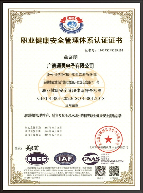
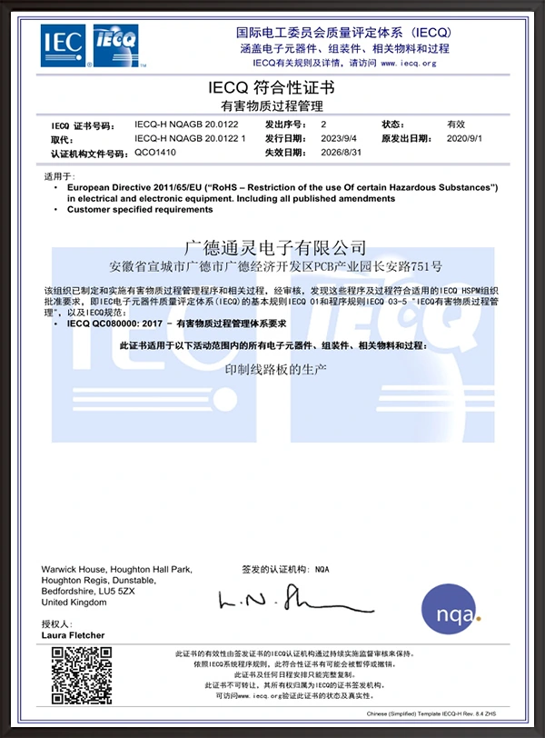
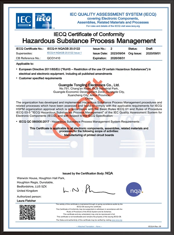
The environmental copy 11426E00850R304 shows 27 April 2026–26 April 2029. The occupational-health copy 11424S24822R1M shows expiry 3 June 2027. The IECQ copies expire 31 August 2026; the English version also carries a “Draft” mark. They are not current hazardous-substance qualification for all catalogue boards.
ISO14001 supplier copyISO14001 supplier copy — read holder, date and scope separately.ISO45001 supplier copyISO45001 supplier copy — read holder, date and scope separately.IECQ Chinese expired copyIECQ Chinese expired copy — read holder, date and scope separately.IECQ English expired Draft copyIECQ English expired Draft copy — read holder, date and scope separately.UL April2019 copyUL April2019 copy — read holder, date and scope separately.UL September2019 metal-base copyUL September2019 metal-base copy — read holder, date and scope separately.Pollutant permit copyPollutant permit copy — read holder, date and scope separately.
FIRST RFQ / BUILD A CONSTRUCTION-SPECIFIC BRIEF
Choose the route, then attach the drawing and acceptance plan.
Stack and substrate: layer structure, grade, copper, dielectric and the thermal or insulation conditions that matter for this order.
Surface and protected areas: solderable finish, contact plating, bevel, peelable-mask regions and assembly conditions.
Manufacturing review: confirm routing and finished holes at the actual stack, special-size use, process route, inspection and electrical coverage.
Commercial and document scope: contracting/producing entity, current material availability, production schedule and the exact required UL/quality construction.
Reviewed 9 October 2026. Twenty-two individual product pages, twenty-three equipment entries, their corresponding original images, the process sheet, dated supplier documents and original official records informed this page. General limits remain separate from individual sample facts.
SOURCE TRAIL
Sources behind this profile
Individual original pages and photographs were read separately. Layer and material facts come from the corresponding title/category; no dimensions, thermal rating or electrical results are estimated from a board photograph. A dated copy or public permit has its stated scope.