Choose the construction and acceptance task before choosing a finish.
广德东风电子有限公司 · Guangde Dongfeng Electronics describes an Anhui manufacturing operation established in 2014, with production beginning in 2016. Its official custom service covers double-sided and multilayer boards, alongside aluminium, ceramic and high-frequency board descriptions. The useful starting point is the captioned catalogue: it separates automotive plugged-hole work, industrial copper requirements, network impedance, connector contacts and RF materials.
The company lists small-batch and non-standard custom work. That service description is not a published minimum order, fixed quick-turn delivery or price. Use the matching example to open a technical enquiry, then agree the order quantity, engineering release and production slot.
ORIGINAL CASE CAPTIONS / NO IMAGE-DERIVED SPECS
Automotive examples pose three different engineering questions.
The following images come from the official Chinese custom catalogue. “Automotive” identifies the manufacturer's application description; it is not evidence of approval by a vehicle brand, a PPAP release or a particular safety class.
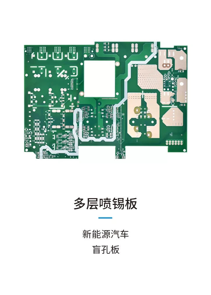
EV multilayer tin-finished blind-via board
Catalogue use
New-energy vehicle
Construction
Multilayer; blind-hole board
Finish wording
Tin spray; lead content not specified
Supply the blind-via stack and filling requirements. Confirm the via formation route, exact tin finish and lead-free requirement before approving a quote.
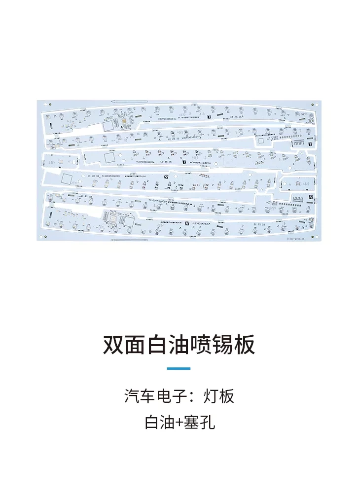
Specify mask reflectance, thickness and colour consistency, plus hole-plug acceptance. The white mask does not establish an aluminium substrate or thermal rating.
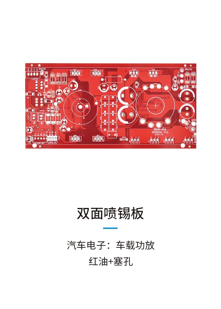
Vehicle amplifier: double-sided tin-finished PCB
Electrical layers
2
Published application
Vehicle power amplifier
Features
Red mask and plugged holes
Confirm the copper distribution, current path and hole-plug plan. Supply the actual laminate and power/thermal acceptance rather than deriving a current rating from the photograph.
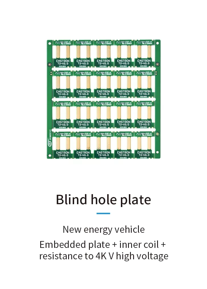
A separate English EV case advertises an inner coil and 4 kV.
Original embedded English EV catalogue image: blind-hole board, embedded board / inner coil and 4 kV wording.
This is a different pictured case, not the Chinese EV board above. The English caption says “resistance to 4K V high voltage”. It does not provide waveform, duration, leakage threshold, insulation distances or a lot-linked test report. For that route, supply the required withstand-voltage test conditions and ask which construction and revision the claim concerns.
COPPER / THICKNESS / HOLE DEFINITION
A heavy-copper label and a numerical copper case are separate evidence.
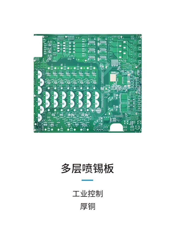
Industrial-control multilayer heavy-copper example
Published application
Industrial control
Copper description
Heavy copper; weight not stated for this example
Finish wording
Tin spray
Ask for finished inner and outer copper and the copper-balanced stack. Do not transfer the separate English 2 oz example to this board.
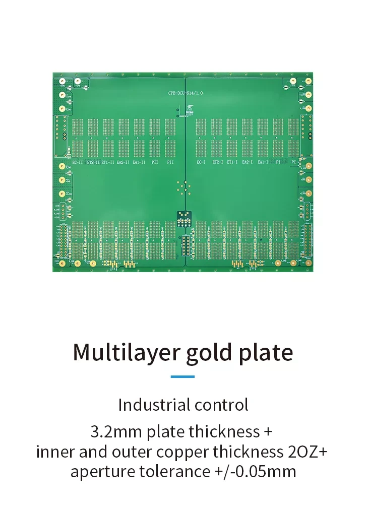
Industrial-control gold board: 3.2 mm / 2 oz
Board thickness
3.2 mm
Copper wording
Inner and outer copper: 2 oz
Aperture tolerance
±0.05 mm; hole definition unspecified
Finish wording
Gold plate; chemistry not defined
Agree whether 2 oz is starting or finished copper, and define the plated finished-hole size. The aperture tolerance does not establish a minimum finished-hole diameter.
The numerical English image explicitly states 3.2 mm board thickness, inner and outer copper 2 oz and aperture tolerance ±0.05 mm. It does not supply an electrical layer count or say whether that aperture is drilled or finished after plating. The separate Chinese heavy-copper image gives no copper weight. Use the numerical case as a conversation starter, not as proof of every heavy-copper construction.
What to attach for industrial-control fabrication
A copper-per-layer stack, with starting foil and required finished copper distinguished.
Finished board thickness, tolerance, hole drawing and plated/non-plated definitions.
Current and thermal requirements for the actual assembly, with any coupon or microsection acceptance.
Panel dimensions, rails, routing/score plan and the dimensional reference used by assembly.
SIGNAL ROUTES / MATERIALS / WEAR SURFACES
Impedance, RF loss and gold-finger wear need different specifications.
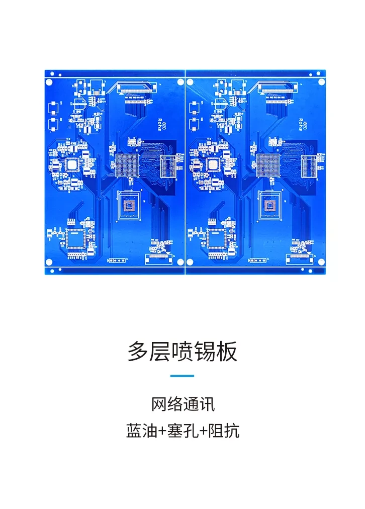
Send the controlled-impedance layer targets, reference planes, coupon drawing and report format. Specify a tolerance in the RFQ; the word impedance alone does not provide one.
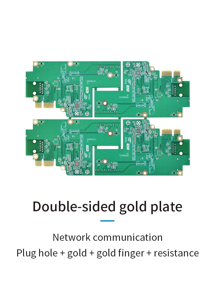
Contact plating and solderable finish require separate definition
Specify connector plating thickness, hardness, bevel and insertion duty, separately from solderable pad finish. Clarify the ambiguous resistance label rather than treating it as a test result.
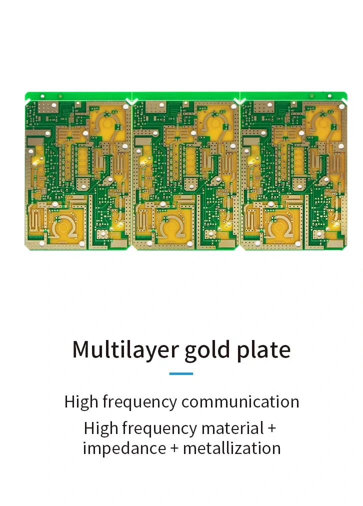
High-frequency communication gold board
Construction
Multilayer
Published features
High-frequency material, impedance, metallization
Laminate grade
Not identified for this pictured board
Request the exact laminate grade, dielectric thickness, copper profile and RF coupon. A general Rogers listing does not identify the material used in this particular example.
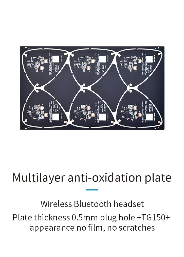
Bluetooth headset: 0.5 mm Tg150 example
Board thickness
0.5 mm
Material wording
TG150; no grade or test method supplied
Features
Plugged holes; anti-oxidation finish
Appearance wording
No film, no scratches
Define Tg measurement/grade, finish chemistry, handling and cosmetic criteria. Confirm what no film means in the quotation, together with acceptance photographs and packing.
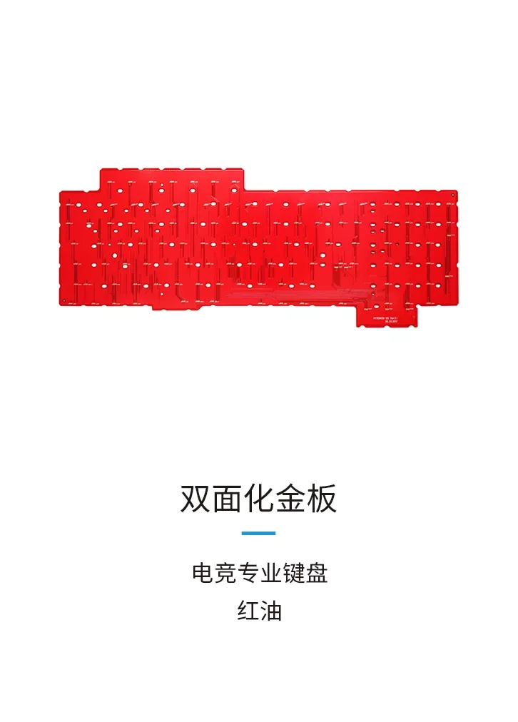
Gaming keyboard: double-sided chemical-gold board
Electrical layers
2
Application
Gaming keyboard
Mask / finish
Red mask; chemical gold wording
Specify the solderable surface finish, thickness and flatness for assembly. The chemical-gold caption does not by itself establish an ENIG process specification or test report.
The general custom menu lists Rogers and PTFE. The RF case itself says high-frequency material without identifying a grade. Request the exact laminate designation and dielectric/copper construction, plus the relevant test frequency and method. An impedance caption gives no numerical tolerance or proof of RF insertion loss.
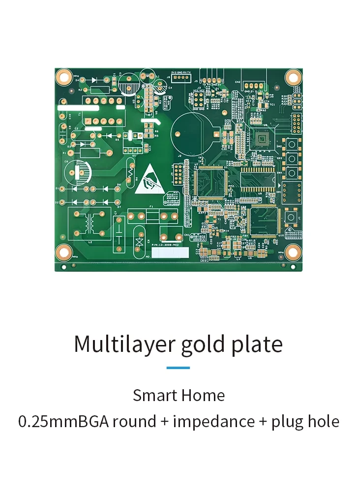
Do not turn “0.25 mm BGA round” into a drilling limit.
Original embedded English smart-home image with the ambiguous 0.25 mm BGA round caption.
The wording does not define whether 0.25 mm refers to a pad, opening, ball-related feature or another geometry. The page does not supply the package footprint or drawing. Send those definitions with your enquiry; this directory leaves trace/space and finished-hole values unknown for that sample.
For the Bluetooth example, the image explicitly pairs 0.5 mm and TG150 with a plugged-hole anti-oxidation board. Specify the laminate grade and Tg method, then clarify “no film” and acceptable scratches. A surface-finish term should not carry unstated storage life or assembly guarantees.
CUSTOM MENU / SEPARATE FROM SAMPLE-SPECIFIC LIMITS
Turn the general menu into a controlled quotation.
Materials and physical stack
Published material classes
CEM-1, CEM-3, FR-4, aluminium-base, Rogers, PTFE
Board thickness menu
0.2–3.2 mm
Copper foil menu
0.5–3 oz; finished-copper definition not given
Maximum processing area
600 × 1200 mm; confirm usable finished-board and panel dimensions
These rows are independent options. They do not establish that the largest panel, thinnest board, highest copper and most complex via stack can be delivered together.
Surface and presentation
Seven finish descriptions
Anti-oxidation; leaded tin spray; lead-free tin spray; contact gold; plated nickel/gold; chemical gold; carbon film
Nickel thickness menu
2–6 μm
Gold thickness menu
0.03–1 μm
Mask colours
Green, black, blue, white, red
Allocate nickel and gold thickness to the particular surface/process. Chemical gold is not a complete ENIG specification; anti-oxidation is not enough to identify OSP chemistry. Define solderable pads and wearing contacts separately.
The website also describes shaped outlines, logo printing, vacuum packing, identification labels and cartons. Confirm rails, bevels, special packaging, shelf/storage requirements and traceability labels against your actual delivery specification.
Where process questions can be directed
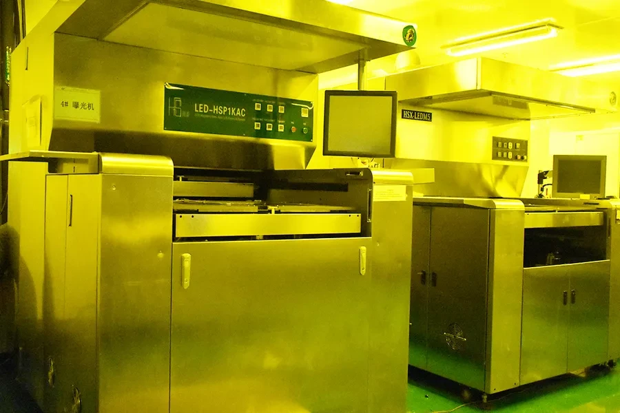
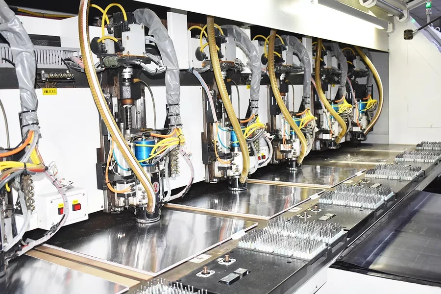
The three equipment pages identify cutting, CCD inner-layer exposure, pressing, six-axis drilling, horizontal PTH and vertical continuous plating; then etching, dry-film application, Xinqi LDI, developing, Optima AOI and board brushing; finally CCD mask exposure, inkjet legend, nickel/gold plating, CNC profiling, automatic electrical testing and final optical inspection. The page headline says 15 processes, while its three screens display 18 equipment/process entries; do not use that headline as an audited route count.
LDI, AOI and electrical-test names are useful points for a quotation review. They do not provide machine availability, laser drilling capability or your order's yield. Request the inspection stage, actual netlist-linked electrical report, coupon data and any process subcontracting for the chosen construction.
ENTITY / SITE / DATED SOURCE RECORDS
Keep the 2014 Anhui company distinct from the 1989 history.
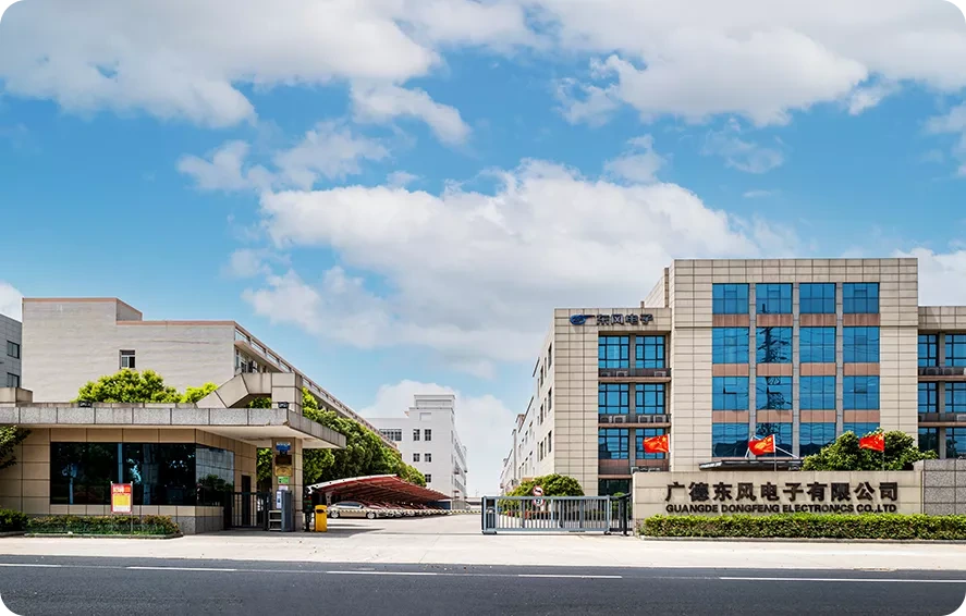
Original company-page photograph of the Guangde Dongfeng entrance and building.
The company page identifies 广德东风电子有限公司 as established in 2014, and its history names 吴江市东风电子有限公司 in 1989. Those are different named entities. The timeline's older UL and SMT milestones do not, by themselves, identify a current Guangde UL holder or prove that today's assembly order runs at this address.
The contact page names No. 749 Chang'an Road, Guangde Economic Development Zone, Anhui. It publishes gddfpcb@vip.163.com and +86 563 6070665. The main contact fax differs from the repeated footer fax; this profile does not select one as verified. The email is an official published 163 mailbox, not a domain mailbox; no control test or message was sent.
The company describes 40 mu of land, 50,000 m² building area and annual capacity of one million m² after two development phases. These undated manufacturer statements are not a current allocation of capacity to your order.
Two dated government-hosted records provide context.
A 10 January 2024 Guangde city page, credited to People's Daily Anhui, reports that Dongfeng exhibited its ceramic-based DBC development on 29 June 2023. That establishes a reported development/exhibition event, not a tested ceramic model, thermal-conductivity value or current mass-production approval. For a ceramic order, ask for substrate type, copper bonding, thermal and isolation test conditions, and the legal entity that supplies it.
The city ecology department's original 8 June 2026 spot-check publication names 广德东风电子有限公司, records a 29 May 2026 check, and states that no problems were found in that listed check. This is a dated environmental inspection entry; it is not PCB quality certification or a guarantee of ongoing compliance for every activity.
Read the actual scope and dates on the published certificate copies
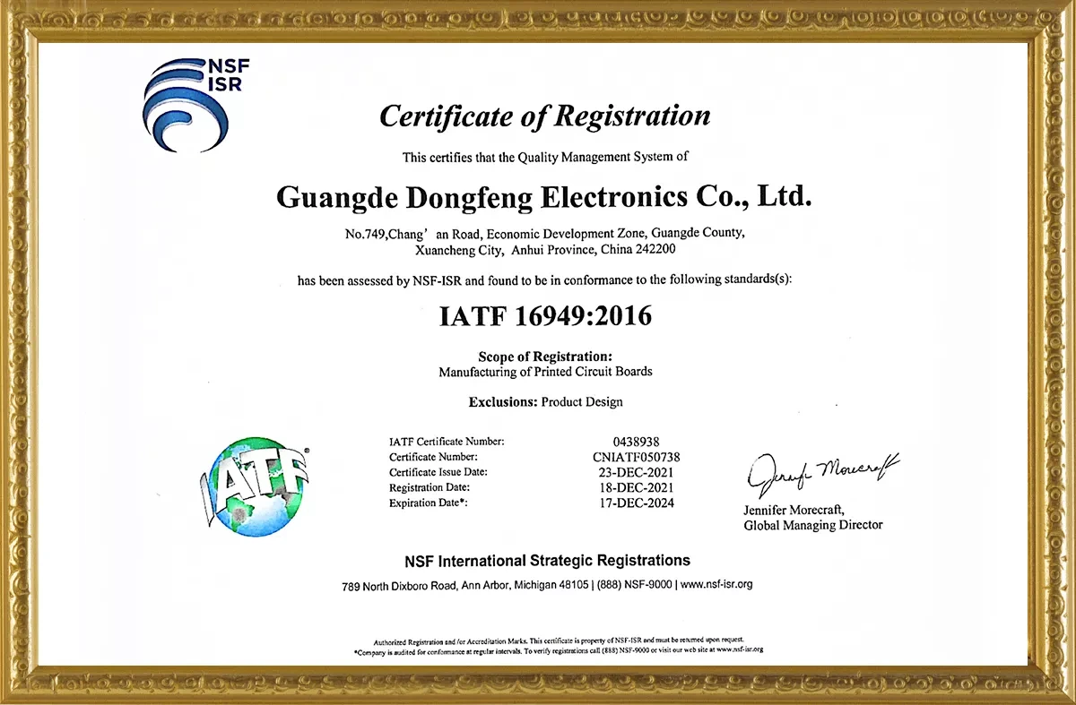
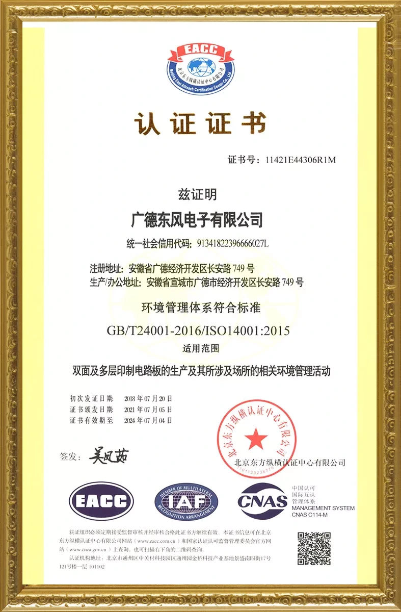
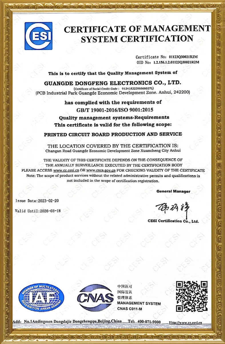
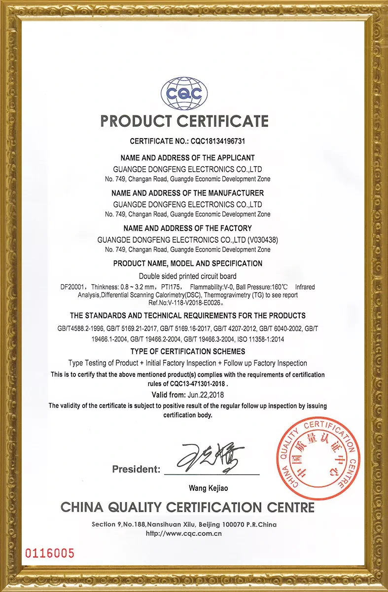
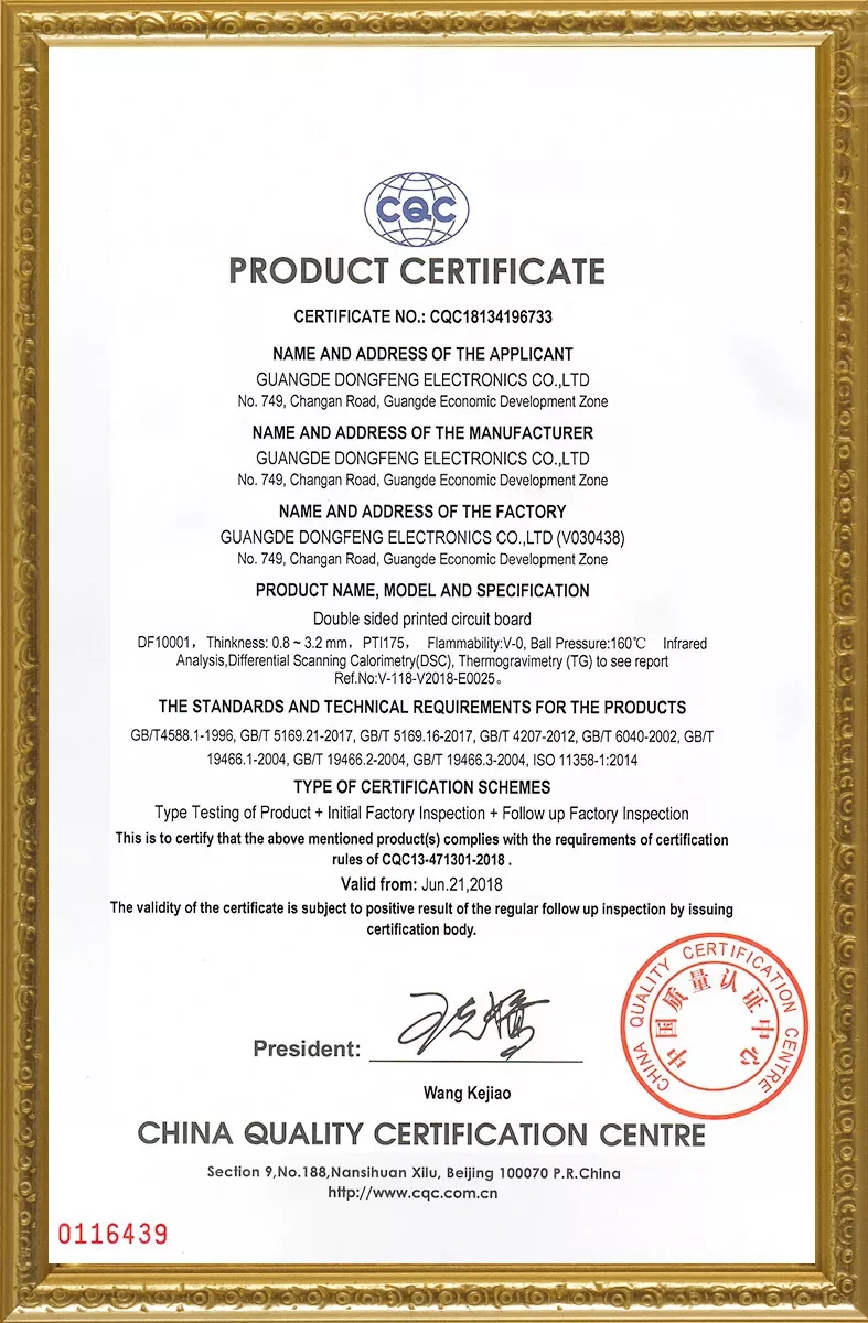
The original pictures below were read individually. Copies establish their printed wording and dates; current issuer status was not queried.
NSF-ISR IATF 0438938 / CNIATF050738: manufacturing of printed circuit boards, product design excluded; issued 23 December 2021, expiry 17 December 2024.
EACC ISO 14001, 11421E44306R1M: environmental activities for double-sided and multilayer PCB production at No.749; expiry 4 July 2024.
CESI ISO 9001, 01123Q30021R2M: PCB production and service; issued 20 February 2023, valid until 18 March 2026.
CQC18134196731 / DF20001 and CQC18134196733 / DF10001: double-sided PCBs, 0.8–3.2 mm, PTI175, V-0 and 160°C ball-pressure wording. The two copies show June 2018 starts and regular follow-up conditions, not a blanket qualification of all pictured boards.
Complete original manufacturer-published certificate copy; printed scope and dates above.Complete original manufacturer-published certificate copy; printed scope and dates above.Complete original manufacturer-published certificate copy; printed scope and dates above.Complete original manufacturer-published certificate copy; printed scope and dates above.Complete original manufacturer-published certificate copy; printed scope and dates above.
SOURCE TRAIL
Sources behind this profile
Individually researched 9 October 2026. Chinese and English corresponding original captions were read separately; sample parameters were not transferred across images. The English page currently exposes little visible text but embeds its captioned originals. Historic certificate copies and government context do not create an independent quality badge. No outgoing enquiry or mailbox-control test was made.