GRANDWORK / HEATING, LIGHTING AND CONTROL CIRCUITS
Choose the thermal or circuit problem before choosing a board.
Grandwork Electronics · 梅州市格兰沃电子有限公司 describes PCB manufacturing established in 2005 in Meizhou's Dongsheng Industrial Park, Guangdong. Its catalogue is broader than an ordinary multilayer-board listing: large etched epoxy heaters sit alongside aluminium-base lighting circuits and FR-4 control boards.
This profile brings together 13 sourcing examples from 23 individually read product pages. Two heater side views and two bulb-board views are grouped with their companion, rather than displayed as duplicate products. The general process chart, equipment gallery and document dates have their own scope below.
EPOXY HEATER / THE PATTERN IS PART OF THE ELECTRICAL DESIGN
Large dimensions do not tell you the resistance or temperature map.
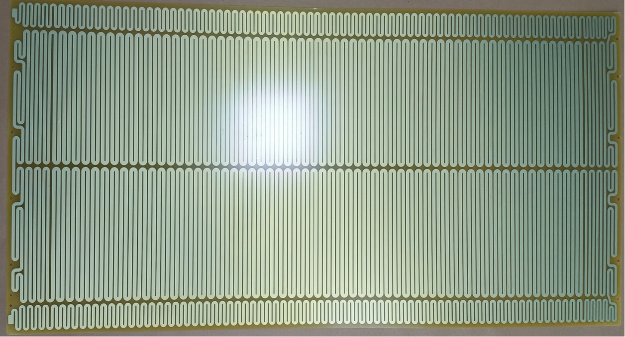
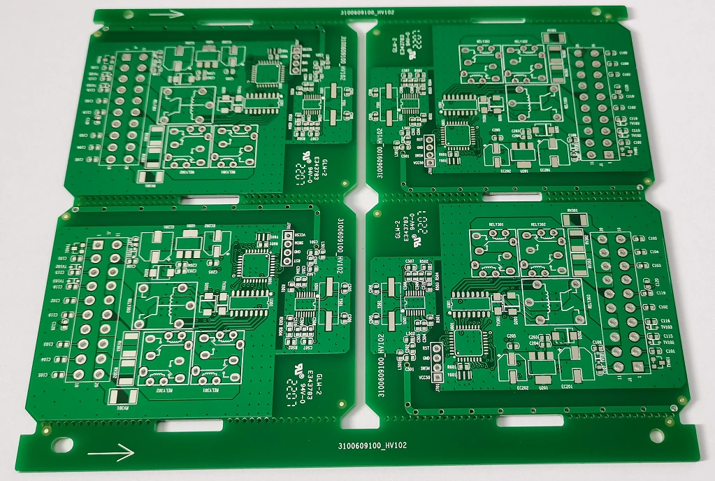
The newer heating-board catalogue shows a green epoxy construction and large etched sheets. Its titles write 700–1450 mm and 665–1400 mm, but do not define whether those numbers describe a dimension pair, a range or a particular usable work area. Send the actual drawing before assuming a maximum finished outline.
Large-format etched epoxy heater
Source title
700–1450 mm large-format epoxy heater etched sheet
Dimension basis
Title does not define a width × length or dimensional range
Insulation wording
DC >10 kV; test conditions not supplied
Release a dimensioned drawing and insulation test voltage, duration and leakage threshold. Confirm usable etching size for this heater route rather than applying the general PCB process-size row.
Green epoxy heating-board example
Construction
Epoxy heating board
Published limits
No resistance, power, temperature or layer figure
Start with the heater drawing, cold/hot resistance and operating voltage, power density, temperature uniformity, lead attachment, mounting and isolation test. The photograph is not a heating-performance result.
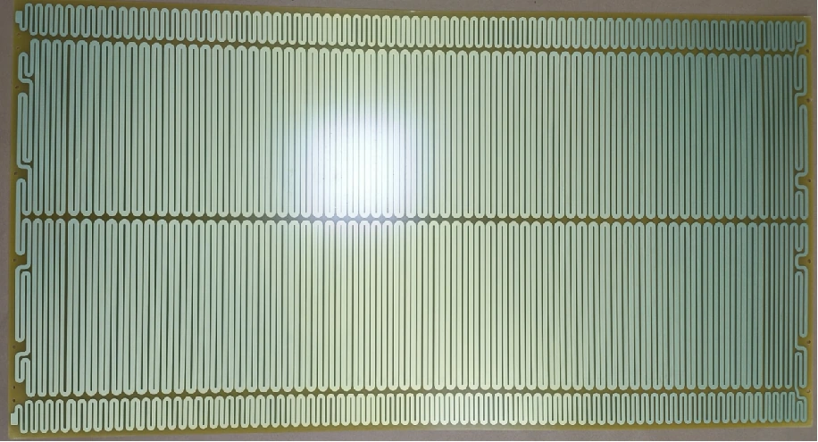
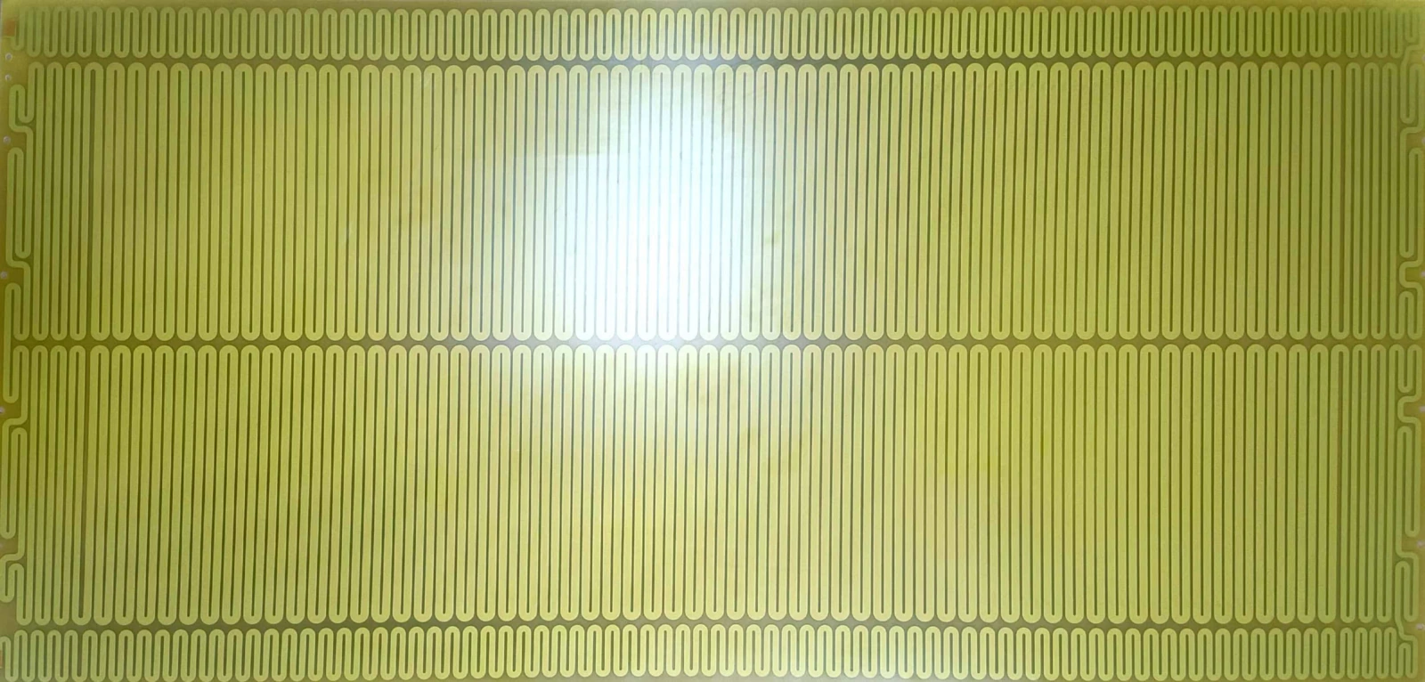
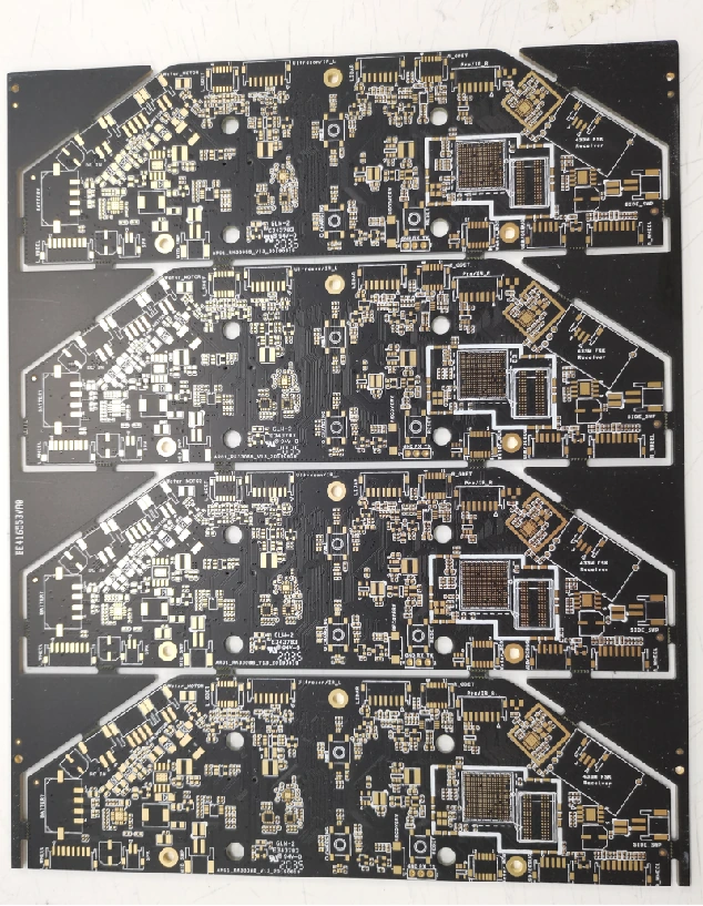
665–1400 mm epoxy heater: two side views
Source title
665–1400 mm soldering side
Companion page
665–1400 mm non-soldering side
Engineering data
No specified resistance, wattage or thermal map
Treat the two pages as side views of a catalogue construction, not two different performance ratings. Ask for copper/resistive pattern, terminals, mounting, permissible hot spots and the released outline.
Companion non-soldering-side view of the separately titled 665–1400 mm heater. It supplies no additional power rating.
ALUMINIUM-BASE CIRCUITS / KEEP THE THERMAL UNIT AND FORMING ROUTE
A lighting board needs an isolation stack, not just an aluminium back.
The indoor and automotive LED examples provide distinct line/space pairs and finishes. Their thermal fields say “1.3W” and “2.0W”, while the tube and bulb pages explicitly use W/m·K. These are different levels of detail; the incomplete units are not silently normalised.
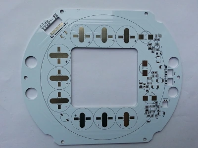
Indoor-LED aluminium-base PCB
Board wording
Aluminium base, 1.6 mm
Copper / finish
1/0 oz / HASL
Line / space
0.4 / 0.5 mm
Thermal field
Source writes 1.3W; denominator undefined
Specify the actual dielectric material and thermal conductivity with units and test basis, aluminium thickness, finished copper and finish requirements. The source’s 1.3W is not published here as W/m·K.
Automotive-LED aluminium-base PCB
Board wording
Aluminium base, 1.6 mm
Copper / finish
1/0 oz / HASL
Line / space
0.3 / 0.4 mm
Thermal field
Source writes 2.0W; denominator undefined
Define dielectric grade, isolation, current and thermal-rise requirements for the actual lamp. An automotive application label and a historical IATF copy do not by themselves approve the vehicle programme.
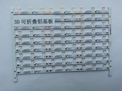
3D foldable aluminium-base PCB
Board wording
Foldable aluminium base, 1.6 mm
Finish
OSP
Line / space
0.3 / 0.3 mm
Bending data
No radius, cycle count or post-forming test
Supply the formed drawing and bend zones, forming responsibility and acceptance after forming. Do not assume dynamic-flex lifetime, standard FPC material or a bend radius from this photograph.
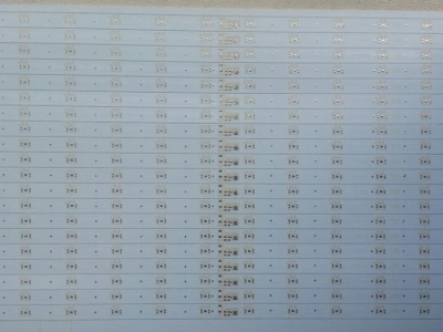
LED-tube aluminium-base circuit
Aluminium-base thickness
0.8–1.5 mm
Copper
1 oz
Thermal conductivity
1–1.5 W/m·K
AC breakdown wording
2–4 kV; test conditions unstated
Distinguish aluminium-base thickness from total finished thickness. Specify laminate grade, dielectric thickness, thermal measurement and finished-board isolation acceptance at the required voltage.
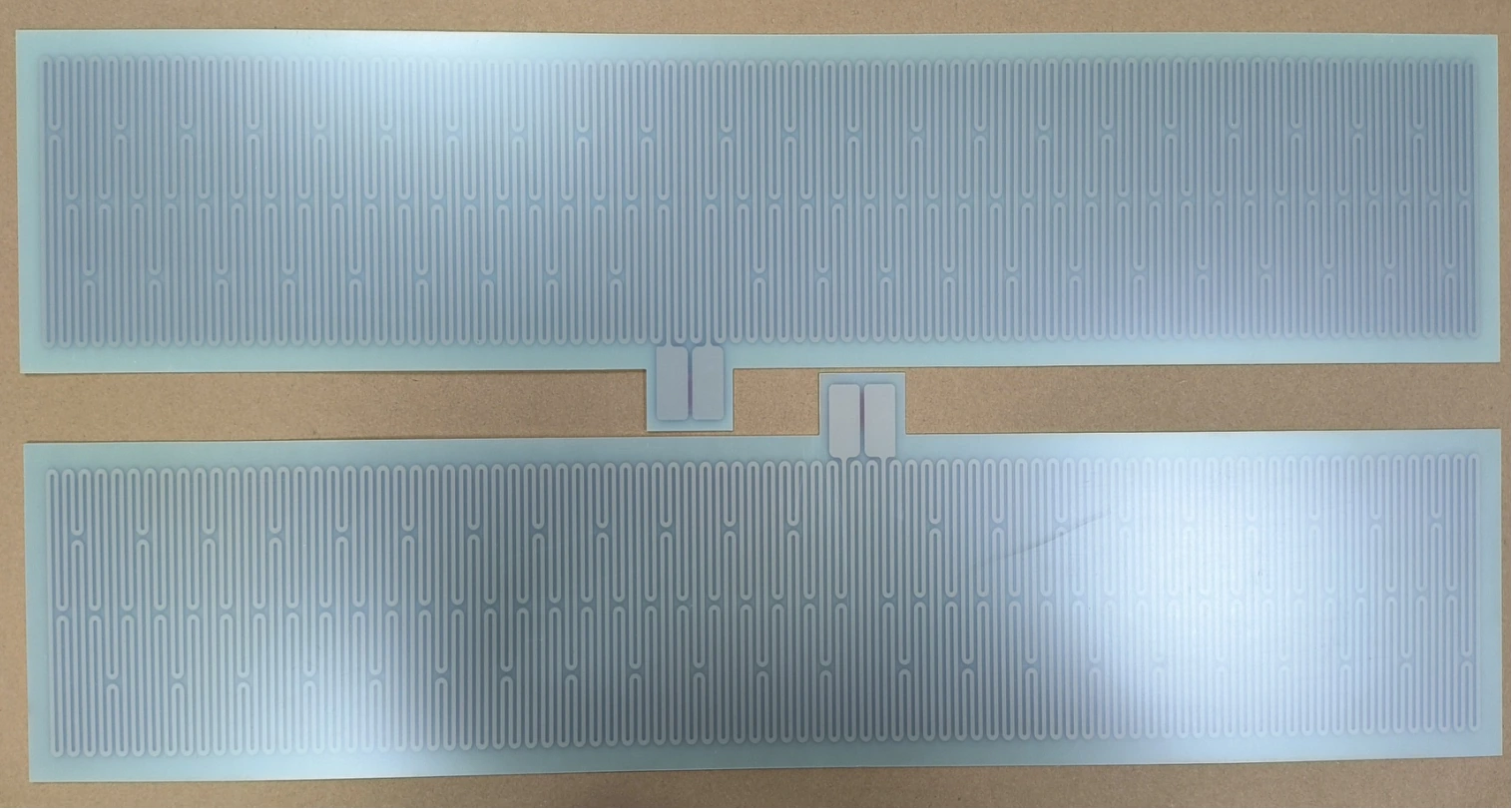
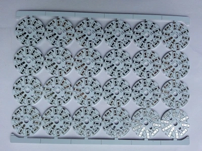
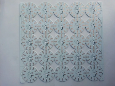
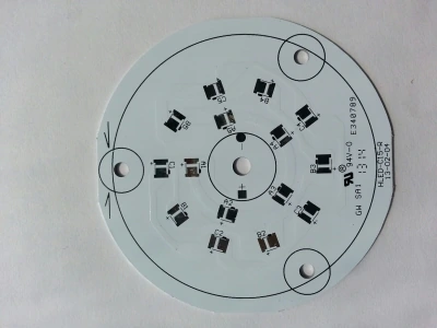
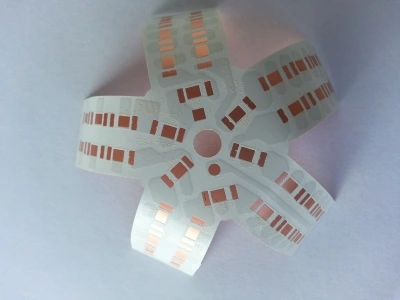
LED-bulb aluminium-base boards: array and individual views
Aluminium-base thickness
1–2 mm
Copper
1–2 oz
Thermal conductivity
1–3 W/m·K
AC breakdown wording
2–4 kV; test conditions unstated
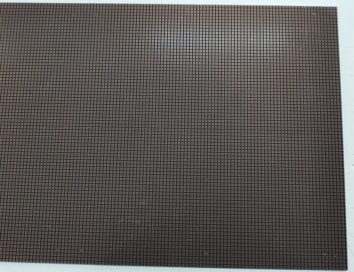
The array and single-board pages publish the same family ranges. Agree panel outline, separation method, dielectric grade and acceptance conditions; a range is not the specification for every array position.
Individual bulb-board view; the companion array page carries the same family ranges. Original 400 × 300 source retained without invented image detail.
FR-4 CONSTRUCTIONS / COMPONENT FEATURES AND SOURCE DISCREPANCIES
Use the product's own stack and line/space.
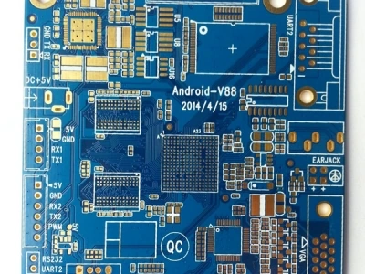
The tablet-board page explicitly identifies four layers and 0.10 / 0.08 mm line/space. Other pages give copper strings without an explicit layer count, or call out “0.2 mm BGA” without defining pitch, pad or hole. Those phrases are not converted into finished-hole minima.
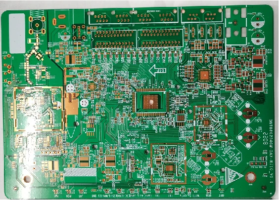
Four-layer tablet motherboard PCB
Layers / thickness
4 / 1.6T source notation
Material
FR-4 TG130–140
Copper / finish
1/1/1/1 oz / immersion gold
Line / space
0.10 / 0.08 mm
BGA wording
0.2 mm BGA; dimensional meaning undefined
Define BGA pitch, pad and escape geometry explicitly, together with the released stack and gold thickness. The 0.2 mm BGA wording is not a finished-hole diameter.
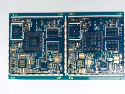
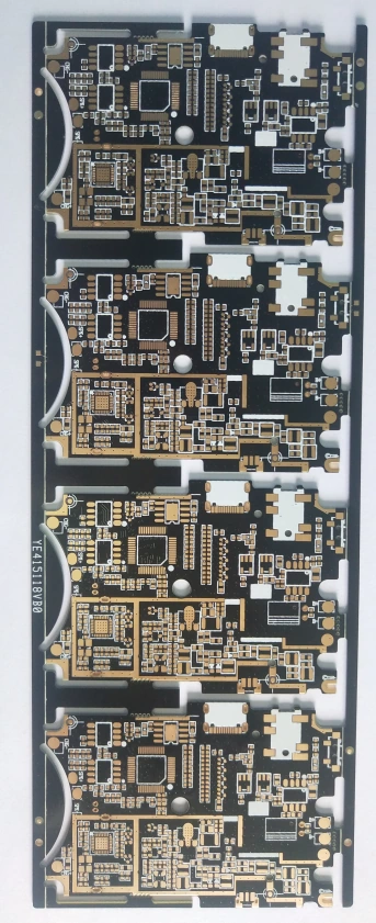
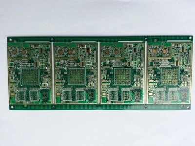
Four-layer half-hole BGA catalogue board
Title
Four-layer half-hole BGA
Summary application
TV display board
Thickness / copper
1.6T / 1/1/1/1 oz
Finish / line-space
Immersion gold / 0.10–0.08 mm
BGA wording
0.2 mm BGA; basis undefined
Resolve the title versus application wording and release castellated-edge details, plating, board edge datum and BGA geometry. The title is retained; no assembly or display performance is inferred.
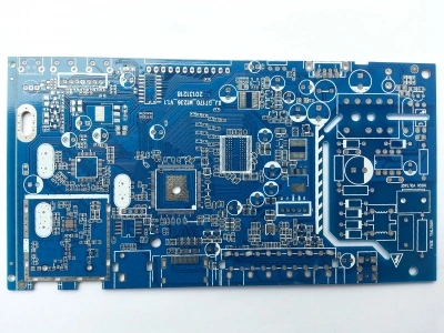
The radio-board page needs a corrected drawing
The summary describes a single-sided, 1.6T, lead-free-HASL board with 0.25 / 0.30 mm line/space. Its detail table describes a four-layer, 1.0T, immersion-gold board with 0.15 / 0.15 mm line/space. Both remain visible below; contradictory layer and line/space fields are excluded from the capability filter.
Radio-board catalogue example with conflicting specifications
Conflicting layer and line/space values are left unset
Request the released radio-board revision, stack, thickness, finish and line/space. The summary and detail cannot both define the same order, so neither has been selected as the confirmed construction.
Taximeter motherboard PCB
Thickness
1.6–2.0T source notation
Copper
1/1/1/1/1/1 oz; layer count not explicitly stated
Line / space
0.127 / 0.127 mm
BGA wording
0.2 mm BGA; basis undefined
Release the actual layer count and stack rather than treating the copper string as an approved stack-up. Define BGA features, finished holes, outline and thickness for the selected design.
Medical-equipment multilayer PCB example
Material / thickness
FR-4 TG150 / 1.2T source notation
Copper
1/1/1/1 oz; layer count not explicitly stated
Finish wording
ROSH LF HAL, as written in the source
Hole wording
Internal-layer minimum hole 0.25 mm; not a finished-hole minimum
Clarify the finish designation, actual stack and internal-hole definition. Specify acceptance and traceability for the device; this application label does not establish ISO 13485 or medical-device certification.
Eight additional application photographs: useful references, no added process limits
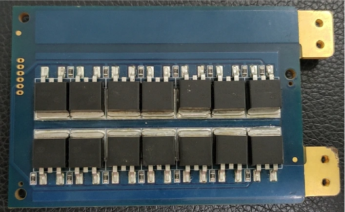
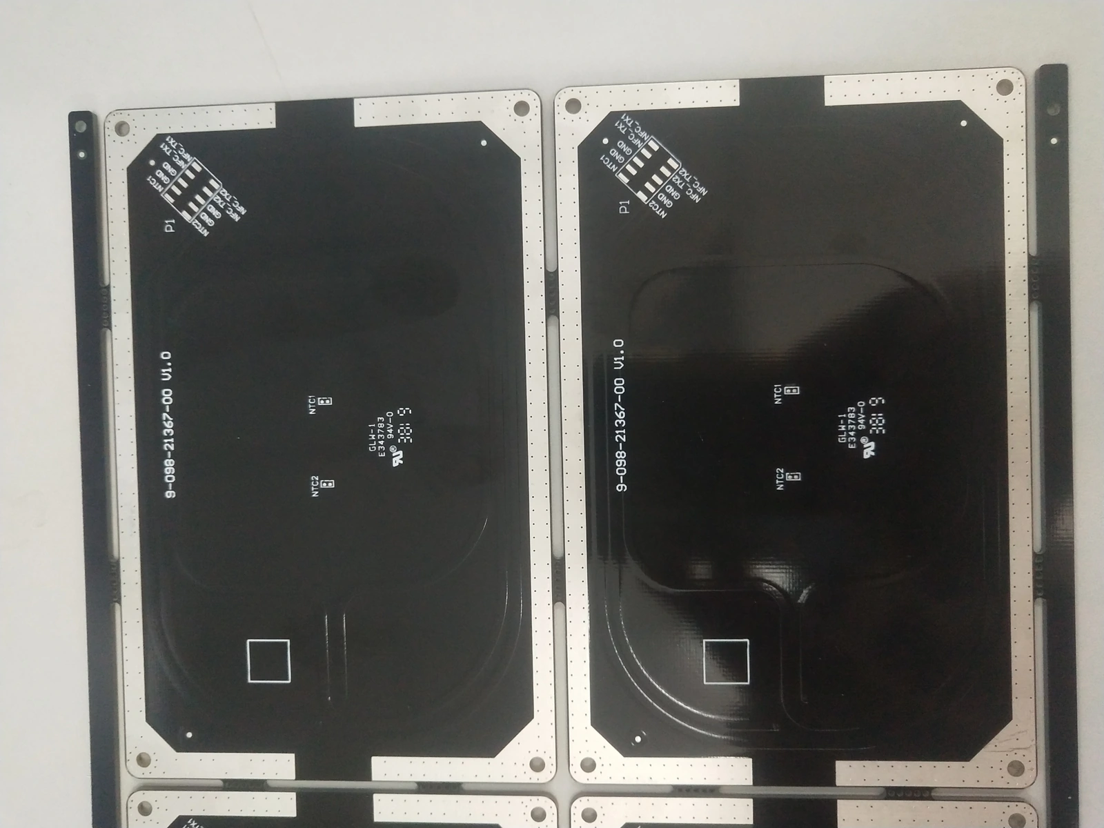
The manufacturer also shows router, wearable, battery-control, LED-display, wireless-charging, remote-control and robot-vacuum boards, plus a thin foldable-board example. Those pages do not publish a usable construction specification. A populated-board photo does not establish an assembly-service scope; the thin-board title does not establish polyimide material or dynamic-flex performance.
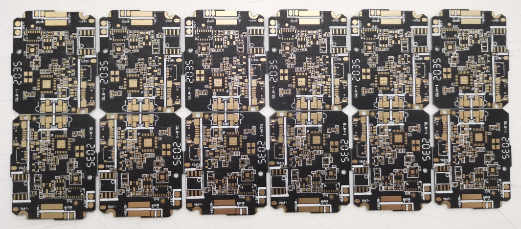
Router motherboardWearable circuitBattery-control applicationLED-display circuitAutomotive wireless-charging applicationRemote-control applicationRobot-vacuum control applicationThin foldable-board example
PUBLISHED PCB WINDOW / SEPARATE ETCHING, DRILLING AND V-CUT
The heater size and V-cut size are different process questions.
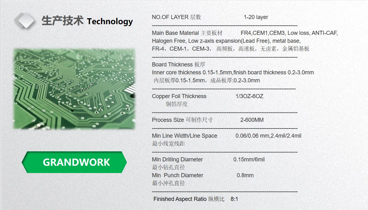
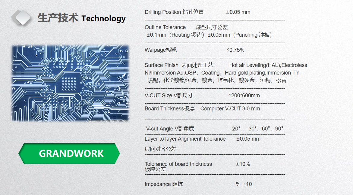
General board chart
Layer range
1–20
Finished-board thickness
0.2–3 mm
Copper
⅓–6 oz
Minimum trace / space
0.06 / 0.06 mm
Minimum drilling diameter
0.15 mm; not a finished plated-hole minimum
Impedance tolerance
±10%; approve geometry, target and test
Mechanical and release details
Outline tolerance
Routing ±0.10 mm; punching ±0.05 mm
Drill position / layer registration
±0.05 mm / ±0.05 mm
Thickness tolerance / warpage
±10% / ≤0.75%
V-cut work size
1200 × 600 mm; maximum board thickness 3 mm
Process-size wording
“2-600MM”; dimension basis unspecified
Aspect-ratio row
8:1; confirm applicable hole and stack
These are individual manufacturer chart rows, not a released 20-layer, 6 oz, 0.06 mm board at the largest size. The heater titles, V-cut machine envelope and ambiguous process-size wording must be confirmed against the actual route. Minimum drilling diameter is not used as the directory's finished-hole filter.
Read the two original capability chartsBoard-process chart; row definitions retained.Mechanical, finish and impedance chart; no combined-limit approval inferred.
PRODUCTION TO LOT RELEASE / SELECT THE REPORT WITH THE BOARD
Choose the test output that resolves your design risk.
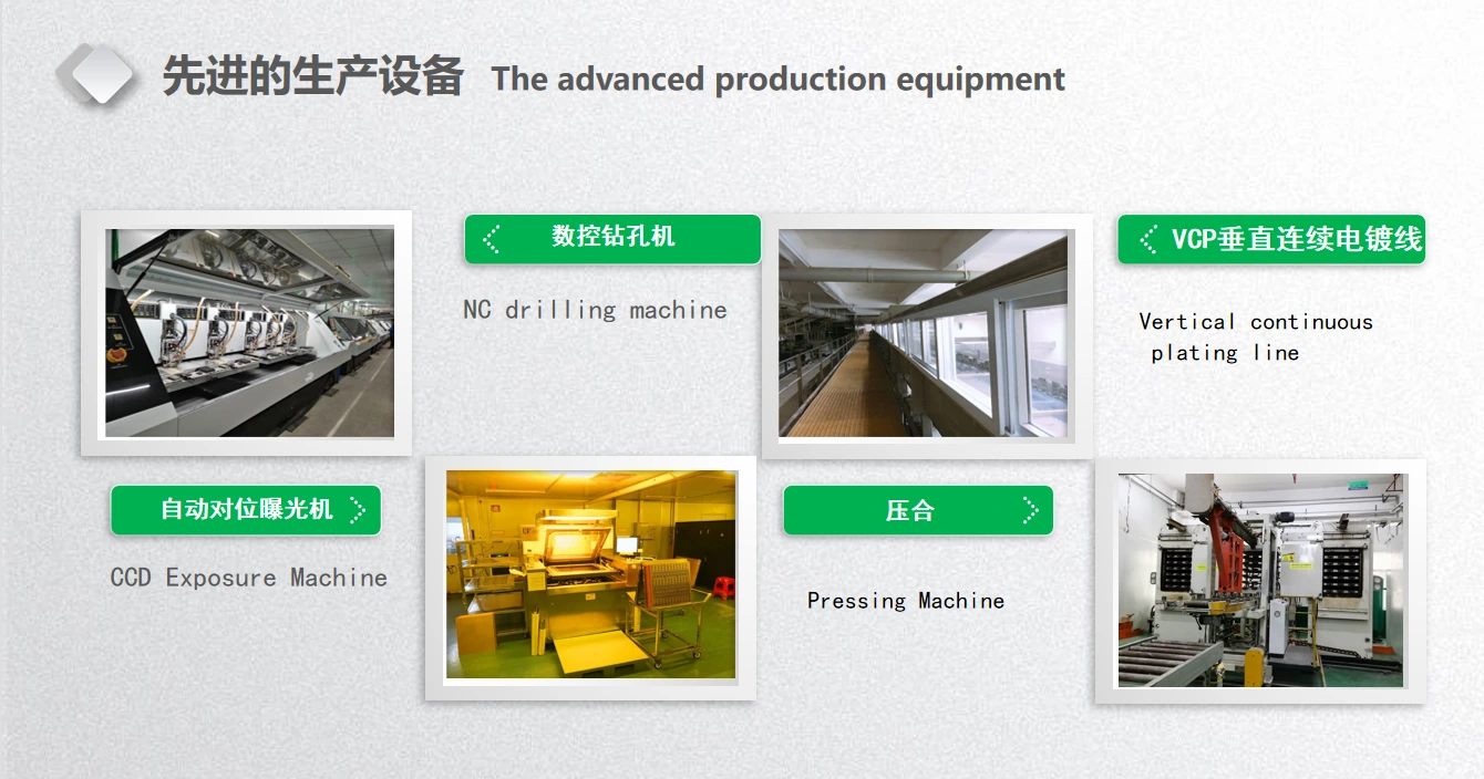
Manufacturer-labelled drilling, continuous plating, CCD exposure and pressing gallery.
Stack and circuit formation
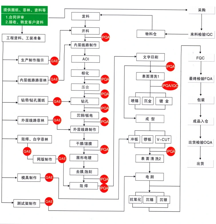
The published process flow links engineering instructions and artwork to inner layers/AOI, lamination, drilling/plating, outer layers, mask, finish, profiling and electrical test. Its equipment list includes CNC drilling/routing, pressing, PTH and VCP lines, AOI, screen printing and finish lines. The undated equipment quantities are not quoted as today's available fleet.
For the selected construction, agree the material lot, stack revision, plating evidence, dimensional datum and which entity performs forming or any subcontracted step.
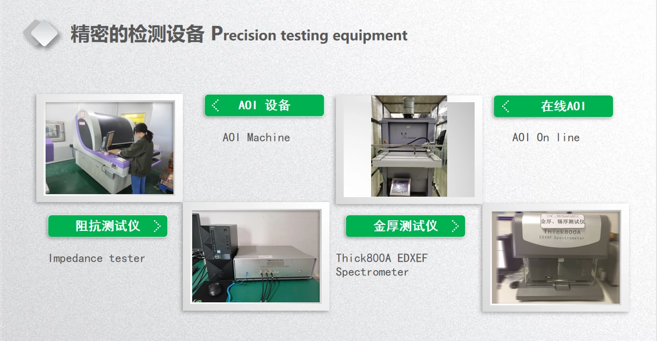
AOI, impedance and coating-thickness instruments, as labelled by the manufacturer.
Impedance, finish and geometry
For a controlled-signal board, define coupon geometry, impedance target/tolerance and the lot-linked report. For plated contacts, agree finish thickness and measurement locations. The instruments shown establish published equipment descriptions, not your order's results.
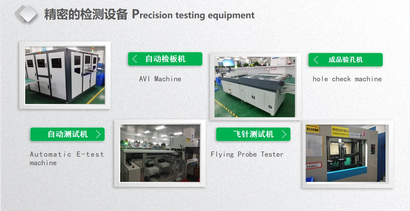
Visual/finished-hole inspection and electrical-test routes.
Continuity, isolation and shipment
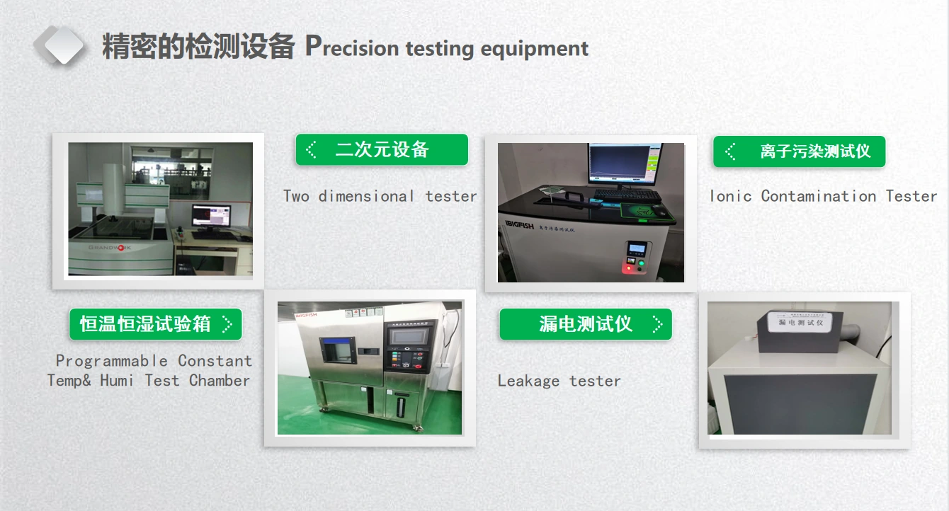
The gallery names fixture electrical testing, flying probe and finished-hole inspection. Another testing sheet names ionic contamination, humidity/temperature, leakage and dimensional instruments. For heaters and metal-base boards, agree test voltage, duration, leakage and post-forming acceptance separately from bare-board continuity.
Request actual pass criteria, sampling and traceability to the supplied engineering revision. The introduction's yield and inspection claims are not converted into an audited rejection rate.
Original engineering-to-shipment flow and environmental-test gallery
Match the supplying entity, plant and current documents.
The contact page places the factory at Dongsheng Industrial Park AD8, No. 1 Development Road 5, Meizhou, Guangdong. It separately lists a Shenzhen operations contact at Villa C9H, TCL International E City, 1001 Zhongshanyuan Road, Xili, Nanshan. Do not treat the Shenzhen contact address as the Meizhou production plant.
Published contacts include +86-755-82712281 and newman@grandwork.net, with sales6@grandwork.net and sales1@grandwork.net also listed. These are transcribed official contacts; mailbox control has not been tested. PCBVerified's RFQ actions remain on this site.
Government identity cross-check and capacity figures
The government-hosted Guangdong 2025 third-batch technology-based SME list names 梅州市格兰沃电子有限公司 at entry 304, page 13, number 2025441402A8014913. This is a dated entity/listing record, not PCB quality approval or a 2026 certification claim.
The company introduction gives over 30,000 m² of workshop and designed monthly capacity of 70,000 m²; the homepage gives over 50,000 m² and 100,000 m². Neither page supplies a reconciled current reporting date. These figures are not combined or used as available production capacity. The introduction's exterior illustration is a rendered building view, so it is not presented here as a factory photograph.
Qualification copies: what the dates actually say
The manufacturer-hosted IATF 16949:2016 copy, NQA T89919 / IATF 0452979, covers circuit-board production, excludes product design and gives validity to 1 July 2025. The ISO 9001 and ISO 14001 copies 39122Q006009R1M / 39122E006002R1M give validity to 9 June 2025. All of those displayed validity dates have passed at this review.
The single-sided CQC copy CQC18134200586 names GLW-CEM1, 0.8–3.2 mm, and validity to 6 July 2025. The separate GLW-1 printed-board copy CQC12134071254, 0.38–3.2 mm, gives validity to 15 September 2026, also before this review. Product-scope limits from these copies are not applied to every catalogue board.
A hosted UL-directory snapshot names GRANDWORK ELECTRONICS CO LTD, E343783, with a last-updated date of 26 October 2018 and separate GLW board types. It is a historical copy; current UL registration and ownership are not established by this page. For a North American order, request a current issuer record for the relevant entity and board type.
The high-tech copy GR202144001632 is dated 20 December 2021 with a three-year validity. The SGS/Made-in-China plaque QIP-ASI1321527 records a 2013-10-18 audit for site existence and business operations, not universal PCB performance. Ask for renewed, applicable documents rather than using these historical copies as current badges.
SOURCE TRAIL
Sources behind this profile
Individually researched 9 October 2026: company/contact and process documentation, 23 original product pages and corresponding complete images, three equipment sheets, five production/test collages, eight dated qualification copies, and the complete government-hosted list with its matching page examined. Product contradictions and undefined units retain their original scope. No combined-limit approval, renewed certification or current available-capacity claim is inferred.