GETONG GROUP / NAMED PRODUCTION AND SALES ENTITIES
Choose the PCB family—and name the factory that will build it.
Getong Electronics publishes six PCB families: double-sided, multilayer, controlled impedance, heavy copper, high frequency and metal base. Its company page names two manufacturing companies, 佛山市格通电子科技有限公司 in Foshan and 惠州市格通电子有限公司 in Huizhou. This PCBVerified record is attached to the Foshan legal entity; the group’s catalogue does not assign each family to a particular plant.
FOSHAN PRODUCTION
Gaoming, Genghe
The contact page gives Zhongxinhua Industrial Park, Baishi Development Zone, Genghe Town, Gaoming District. The history page dates the Foshan company to April 2013.
HUIZHOU PRODUCTION
Zhongkai, Tongqiao
The contact page gives No. 29, south side of Lianfa Avenue, Tongqiao Town, Zhongkai High-Tech Zone. The history page dates the Huizhou company to August 2008.
Keep the sales entity separate from the producing site.
The same contact page lists Getong’s Hong Kong company at Room 1905, Nam Wo Hong Building, 148 Wing Lok Street, Sheung Wan, and Shenzhen Jiachuanhui at Qunxing Plaza A2608, Huaqiang North Road. The history calls them international and Shenzhen sales branches. Confirm the entity signing the purchase order, the plant doing fabrication and the party issuing quality records; a group sales address is not a fabrication address.
Group founding in 2008 should not be read as the Foshan company’s incorporation date. The official history distinguishes the entities. The original Guangdong 2021 first-batch high-tech-enterprise list, hosted by Puning’s government, names the Foshan company at row 1664 with GR202144002669. It is a historical identity/recognition record, not current PCB certification.
CATALOGUE FAMILY ENVELOPES / 0.10 MM PATTERNING
Compare double-sided, multilayer and impedance requirements separately.
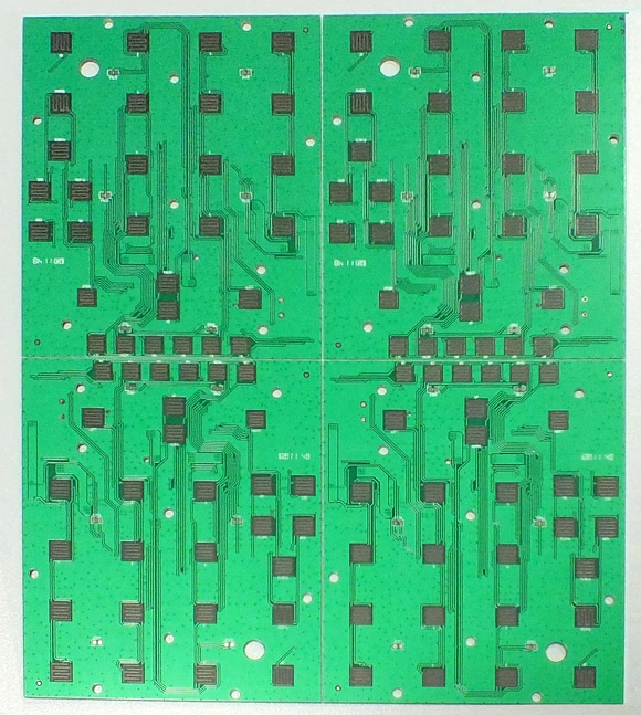
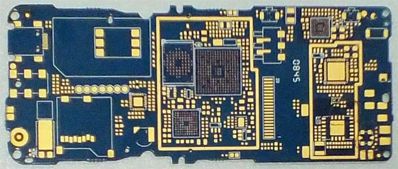
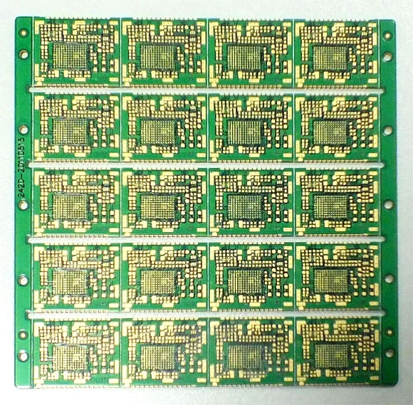
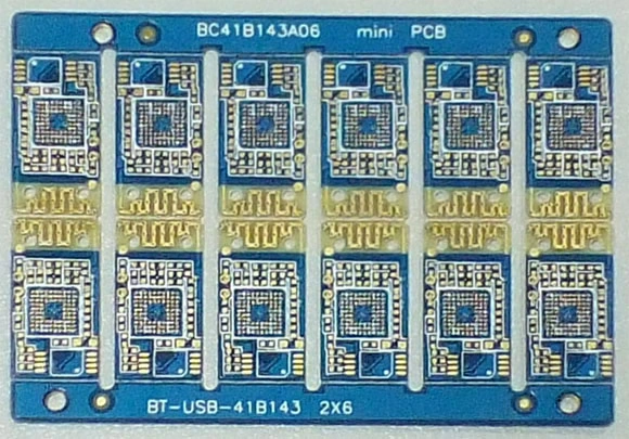
The individual product pages give construction-family ranges alongside their original photographs. The listed envelope is not the measured build specification of the pictured sample. Double-sided work is explicitly two layers; multilayer and impedance families list 4–10 layers. Their 0.10 mm trace and 0.10 mm spacing entries remain separate from the coarser specialty-family entries below.
Double-sided
CEM-3, FR-4 and high-Tg FR-4 are listed, with 0.3–3.2 mm finished thickness. Select the actual grade and copper; these materials are not interchangeable without design approval.
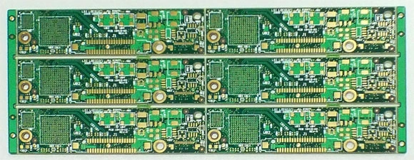
The three separate examples share a 4–10-layer family envelope and 0.4–3.2 mm finished thickness. Request the actual press stack and the plant performing lamination.
The family page gives 4–10 layers and 0.3–3.2 mm thickness, but no numerical impedance tolerance. Supply the target, approved stack, coupon and delivered measurement record.
Minimum hole 0.20 mm; drilling versus finished size not defined
Confirm CEM-3 versus the selected FR-4 grade, finished copper, plated/non-plated hole definitions and electrical-test coverage for the drawing.
Turn the family envelope into a drawing approval.
For an ordinary two-sided board, freeze material, finished copper, mask openings, plated and non-plated holes, outline and netlist. For a multilayer design, add layer order, dielectric thicknesses, copper balance and any controlled-impedance zones.
The pages list “minimum hole 0.20 mm” without saying whether that means drill tool or finished diameter. We retain it in the source facts, but do not enter 0.20 mm as a verified finished-hole filter value. Ask the fabricator to approve finished PTH and NPTH dimensions separately.
Multilayer PCB catalogue: first example
Published family
4–10-layer family
Family board thickness
0.4–3.2 mm
Family trace / space
0.10 / 0.10 mm
Source hole wording
Minimum hole 0.20 mm; drilling versus finished size not defined
Confirm the selected layer count, stack symmetry, glass/resin system and press construction. Ask which producing site will perform lamination and electrical testing.
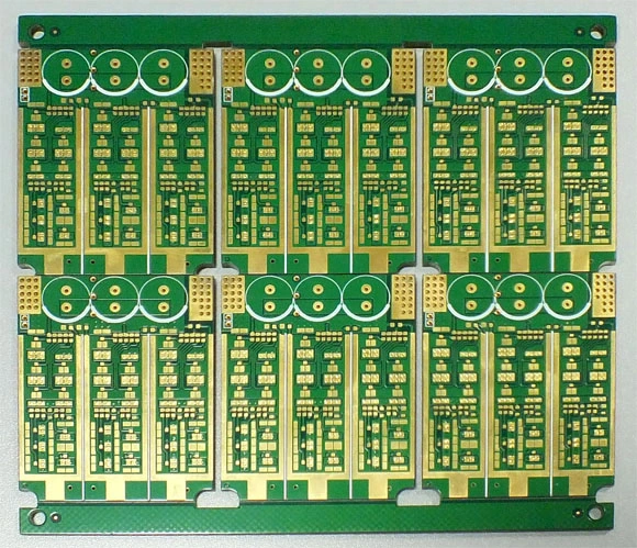
Multilayer PCB catalogue: second example
Published family
Second separately pictured multilayer example
Family board thickness
0.4–3.2 mm
Family trace / space
0.10 / 0.10 mm
Source hole wording
Minimum hole 0.20 mm; drilling versus finished size not defined
Release panel rails, finished outline, drill map and netlist. The shared family envelope does not specify the finished dimensions or hole definition of this panel.
Multilayer PCB catalogue: third example
Published family
Third separately pictured multilayer example
Family board thickness
0.4–3.2 mm
Family trace / space
0.10 / 0.10 mm
Source hole wording
Minimum hole 0.20 mm; drilling versus finished size not defined
Specify edge contacts or local finish zones in the drawing if required, alongside the accepted stack, copper and test records. The image does not establish a contact plating thickness.
Controlled-impedance PCB catalogue
Published family
4–10-layer family; no numerical impedance tolerance published
Family board thickness
0.3–3.2 mm
Family trace / space
0.10 / 0.10 mm
Source hole wording
Minimum hole 0.20 mm; drilling versus finished size not defined
Provide the target impedance, tolerance, stack and coupon requirement. Ask for the measurement method and shipment record; the family title supplies no ±5% or ±10% promise.
Specify the impedance result you need.
Include single-ended/differential targets, tolerance, reference planes, coupon location and test method. Ask whether the reported value will be measured on coupons, calculated from the proposed stack, or both.
Neither the catalogue title nor the old general table’s “impedance test: yes” supplies a ±5% or ±10% guarantee. Keep the order’s electrical acceptance criteria explicit.
THICK-COPPER FAMILY / COPPER-CONDITIONED ARTWORK
Release the copper distribution before agreeing fine features.
FINISHED COPPER2–6 oz
Published heavy-copper family statement; inner/outer assignment is not given.
LAYER FAMILY2–10
Separate from the stack of either pictured panel.
TRACE / SPACE0.20 / 0.20 mm
The family entries are coarser than the 0.10 mm rigid-family entries.
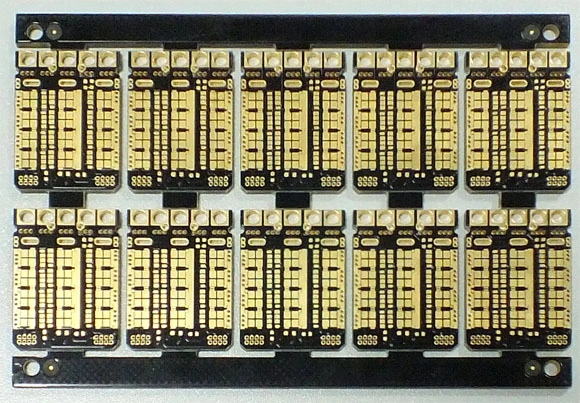
The heavy-copper pages list 0.6–3.2 mm finished board thickness and FR-4/high-Tg FR-4 alongside Rogers, Teflon and Taconic wording. Request a precise laminate grade and copper schedule. A list of possible materials is not an approved mixed-material stack or evidence that 6 oz copper can use every listed minimum feature simultaneously.
Heavy-copper PCB catalogue: first panel
Published family
2–10-layer family; finished copper 2–6 oz
Family board thickness
0.6–3.2 mm
Family trace / space
0.20 / 0.20 mm
Source hole wording
Minimum hole 0.20 mm; drilling versus finished size not defined
Specify finished inner and outer copper separately. Request an approved trace/space and etch-compensation rule for the chosen copper weight, rather than combining 6 oz with every minimum entry.
Heavy-copper PCB catalogue: second panel
Published family
Second original panel; same published 2–6 oz family
Family board thickness
0.6–3.2 mm
Family trace / space
0.20 / 0.20 mm
Source hole wording
Minimum hole 0.20 mm; drilling versus finished size not defined
Agree the thermal/current design, hole-wall copper, soldering exposure and inspection evidence. The listed power and industrial uses do not supply a current rating for this photographed panel.
RF DIELECTRIC AND METAL-BASE ISOLATION ARE DIFFERENT DECISIONS
Select the material by part number, not by family name.
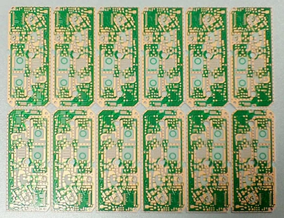
High-frequency PCB catalogue
Published family
Single-sided to six-layer RF family
Family board thickness
0.5–3.2 mm
Family trace / space
0.20 / 0.20 mm
Source hole wording
Minimum hole 0.20 mm; drilling versus finished size not defined
Name the exact laminate grade, dielectric thickness, copper profile and frequency assumptions. Request the approved stack and relevant coupons; brand names do not specify insertion loss.
High-frequency construction
The RF catalogue names Teflon, Rogers, Arlon, Taconic and F4Bk, with single-sided to six-layer construction, 0.5–3.2 mm thickness and 0.20 mm trace/space. It does not give a laminate grade, Dk/Df, copper roughness or RF loss measurement for the pictured panel.
Specify frequency, laminate part number, dielectric and copper thickness, controlled geometry and the test deliverables. Confirm the supplying plant and any mixed-stack construction. The image is not evidence of a particular microwave performance.
Metal-base construction
The metal-base pages list single-sided to six layers, 0.8–3.2 mm thickness and 0.20 mm trace/space. The material field literally says “Burgquist, Ruikai”. That spelling is kept as source wording; it is not silently corrected into a certified brand relationship or a qualified grade.
Give the metal substrate, dielectric part number and thickness, thermal conductivity, isolation/breakdown requirement, mounting interface and finished outline. The pages provide no W/m·K value. Identify which of the family’s layer constructions is intended before using either example as a quotation reference.
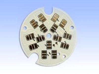
Metal-base PCB catalogue: round example
Published family
Single-sided to six-layer family
Family board thickness
0.8–3.2 mm
Family trace / space
0.20 / 0.20 mm
Source hole wording
Minimum hole 0.20 mm; drilling versus finished size not defined
Specify the metal substrate, exact dielectric grade, thermal conductivity, breakdown requirement and mounting interface. The original material spelling is not silently converted into a qualified supplier or a part number.
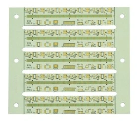
Metal-base PCB catalogue: panel example
Published family
Separate original metal-base panel; same family specification
Family board thickness
0.8–3.2 mm
Family trace / space
0.20 / 0.20 mm
Source hole wording
Minimum hole 0.20 mm; drilling versus finished size not defined
Release the finished outline, mounting-hole insulation, solder-mask openings and depanelisation method. Determine which of the family layer choices applies to the ordered construction.
READ THE COLUMN AND THE DOCUMENT OWNER
The legacy roadmap is a question for engineering, not a current limit table.
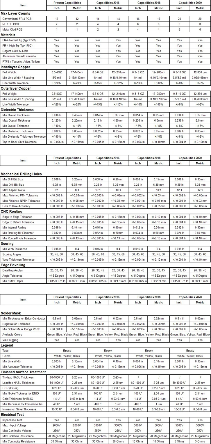
The technical image has columns titled Present Capabilities, Capabilities 2016, Capabilities 2018 and Capabilities 2020. Its Present column gives conventional FR-4 maximum 12 layers, RF/HF 2 layers and metal-clad 1 layer; later columns extend those figures. The original chart is available below, but a year label does not establish that the planned capability was implemented or that it is current in 2026.
Reconcile the family and the table.
Individual catalogue pages name RF/metal families up to six layers and heavy copper up to 6 oz. The old Present column has narrower RF/metal layer entries and 0.5–4 oz inner/outer foil ranges. Ask which current plant-specific rule set applies; do not combine the most favourable number from each source.
Check the document identity.
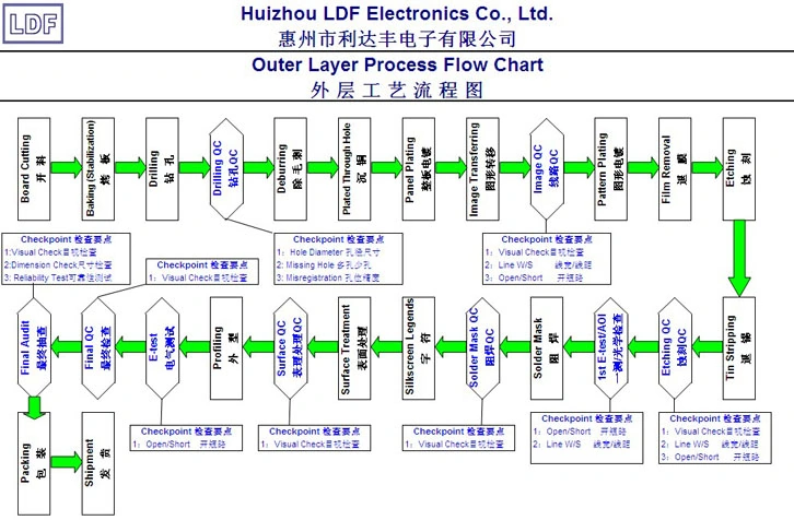
Both inner/outer process flowcharts on the site are headed Huizhou LDF Electronics Co., Ltd. / 惠州市利达丰电子有限公司. The reviewed Getong history does not establish that company’s relationship to the named Foshan/Huizhou Getong entities. These charts are not represented as proof of Getong’s current process ownership.
Do not invent a capacity unit.
The capacity graph gives 6,000 / 4,000 / 3,000 / 1,000 / 500 for 2/4/6/8/10-layer categories, without a unit or period. It is not converted into monthly m² capacity or a promise of available slots.
Read the original roadmap and the document-owner conflict
Original technical image: Present and separate 2016/2018/2020 columns
Approve a current route-specific specification.
The old Present column distinguishes a 0.20 mm drill bit from finished PTH tolerance ±0.08 mm and NPTH tolerance ±0.05 mm. A drill-tool minimum is not a finished-hole guarantee.
Its mask-bridge row includes tolerance signs, and several imperial/metric values require interpretation. Request the current controlled process specification rather than treating an ambiguous old image as an automatic pass for the artwork.
Original outer-layer flowchart is explicitly headed Huizhou LDF Electronics
CATALOGUE EQUIPMENT / ORDER-SPECIFIC OUTPUT
Ask what is inspected, and which report ships with the board.
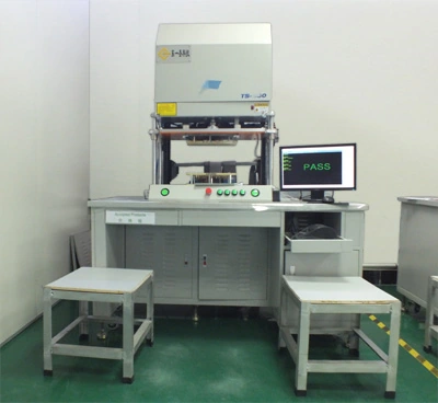
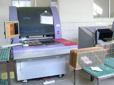
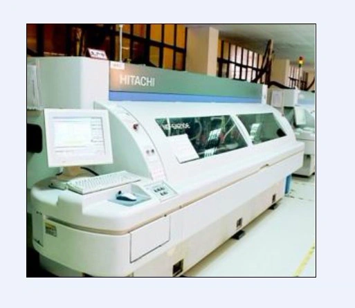
The manufacturer’s equipment pages separately identify electrical testing, AOI, automatic plating, microscopy, lamination, DES, CNC drilling, flying-probe testing, copper deposition/desmear and exposure. The following photographs are paired with named equipment entries. A catalogue photograph does not establish its current allocation, calibration or test coverage for the order.
Manufacturer-labelled electrical test equipmentManufacturer-labelled AOI equipmentManufacturer-labelled CNC drilling equipment
Quote the complete release package.
Selected family, drawing revision, layer stack, laminate grade and finished copper by layer.
Finished outline, panel arrangement, plated/non-plated holes, mask and surface-finish zones.
Electrical netlist, impedance/coupons or thermal/isolation tests where applicable, acceptance criteria and delivered reports.
Contracting company, producing site, externally performed steps, current qualification scope and dispatch date.
Agree the rush route in writing.
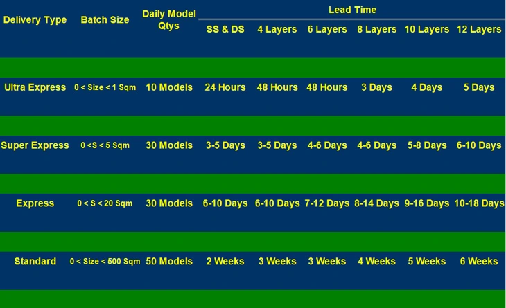
The old lead-time chart’s Ultra Express row is limited to 0 < area < 1 m², with 24 hours for single/double-sided, 48 hours for four/six layers, 3 days for eight, 4 days for ten and 5 days for twelve. These are published legacy schedule entries, not reserved production slots.
The same chart has distinct <5 m², <20 m² and <500 m² bands. Request a current quote identifying area definition, material availability, engineering release, testing and dispatch. Do not infer a present 12-layer service commitment from this schedule alone.
View the original area-dependent lead-time chartOriginal legacy schedule: separate area bands, layer counts and model quantities
The homepage still uses older ISO/TS standards, and no current certificate-holder/type check was established in this review. If your programme requires UL, ISO or automotive qualification, ask for the current issuer-verifiable document and the producing-site scope before approving the purchase order.
SOURCE TRAIL
Sources behind this profile
Individually researched 9 October 2026: company history, contacts, ten individual catalogue pages and original images, technical/schedule/process charts, named equipment and original government list. Family ranges are not sample measurements. Legacy document ownership and column dates are preserved; finished-hole and impedance values remain unknown where the source does not define them.