FUJIAN YONGSHENG / FROM SAMPLE TO MANUFACTURING INSTRUCTION
A Fuding PCB catalogue that needs a drawing-specific release.
Fujian Yongsheng Electronics / 福建永盛电子有限公司 presents PCB manufacturing and SMT services from Wendu Industrial Area in Fuding, Fujian. Its official gallery contains 18 numbered board samples. A few labels identify meaningful particulars: six layers, high-frequency material, 0.10 mm line/space or a multilayer construction. The remaining photographs are useful references, but do not specify an application, stack or finished copper.
For bare-board sourcing
Compare the four documented sample references below, then use the layer-conditioned process table to open a feasibility review. Agree the complete stack, finished geometry, material and inspection on the drawing.
For assembled supply
The company introduction includes SMT. The reviewed gallery does not identify a complete assembly line, component-size envelope or functional-test coverage. Request the assembly site and scope, BOM, placement file and test procedure separately from the PCB quotation.
The sample pages date from 2014 to 2019. They are historical catalogue references, not a promise of an unchanged production recipe or current spare capacity. Selecting one for RFQ means referencing that construction for discussion, not buying the photographed panel as a standard stocked item.
CATALOGUE DESK / MATCH THE SOURCE TO THE BOARD
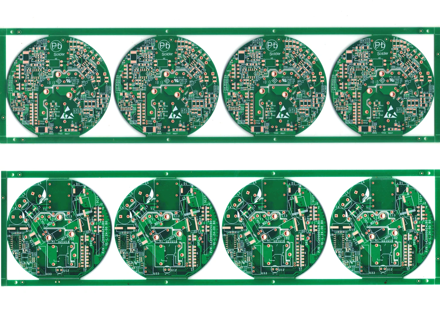
Six layers, high-frequency material and fine routing are separate examples.
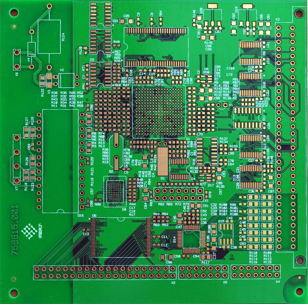
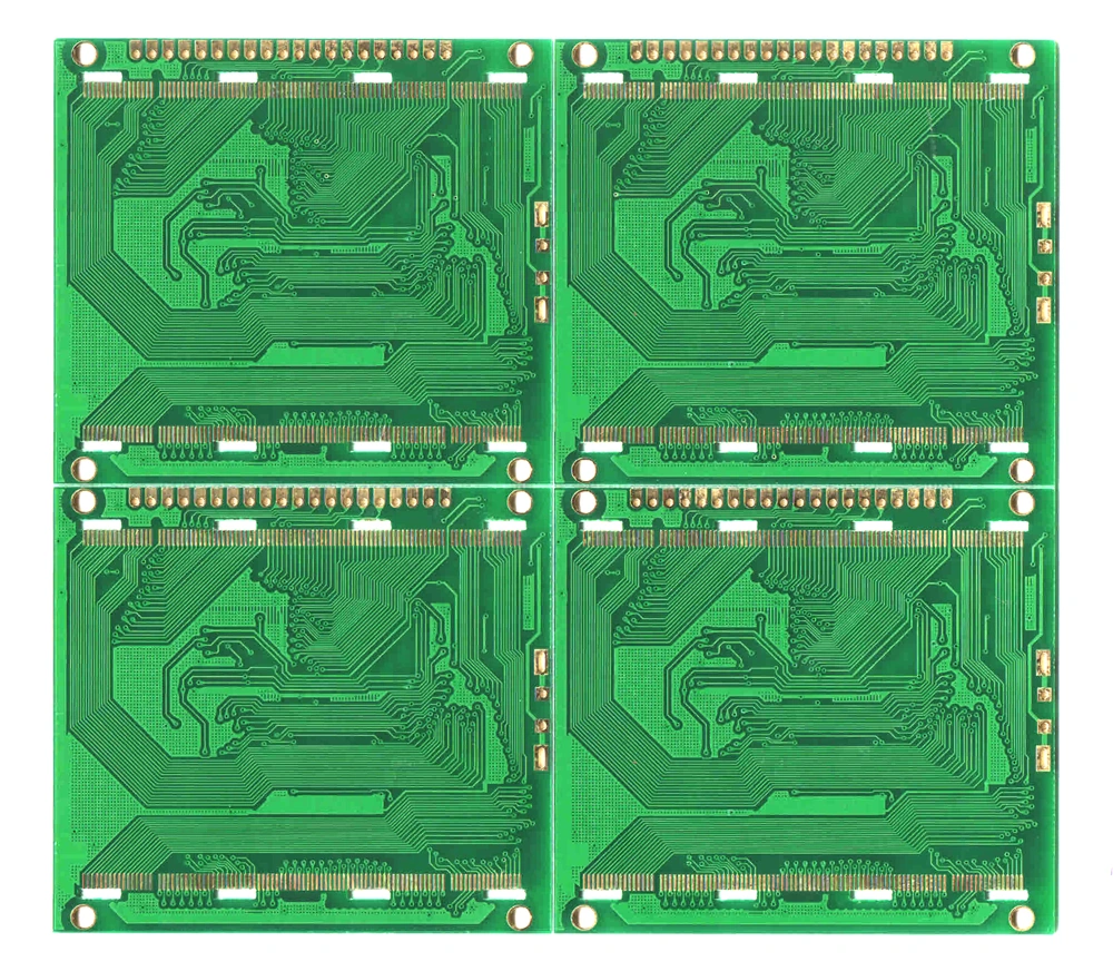
Six-layer PCB — official sample 7 — original catalogue photograph.
Six-layer PCB — official sample 7
Catalogue identification
Sample 7
Layer count
6 layers
Published
20 September 2014
Material / thickness / finish
Not specified for this sample
Request the six-layer stack, finished thickness, reference planes and impedance acceptance. The general 1.00–3.00 mm range for 6–8 layers is a planning limit, not this sample’s disclosed thickness.
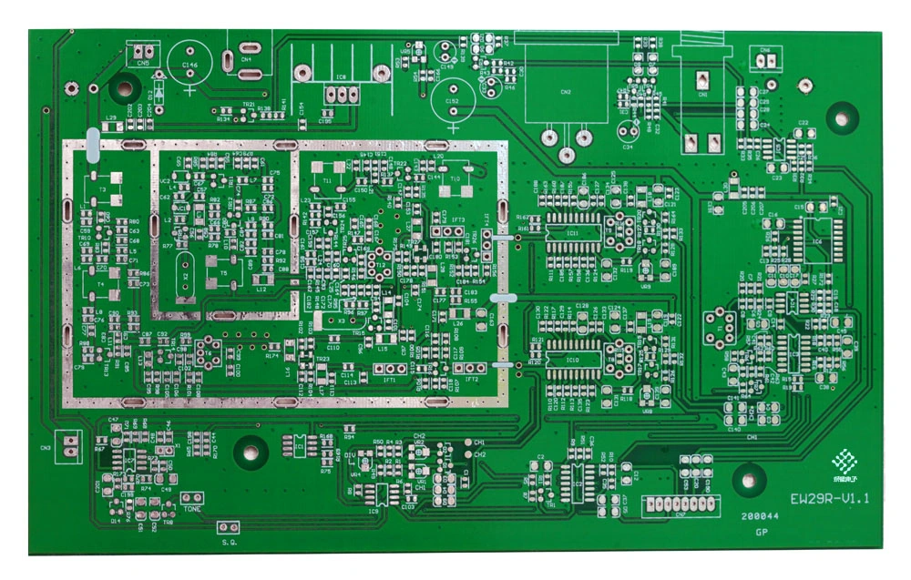
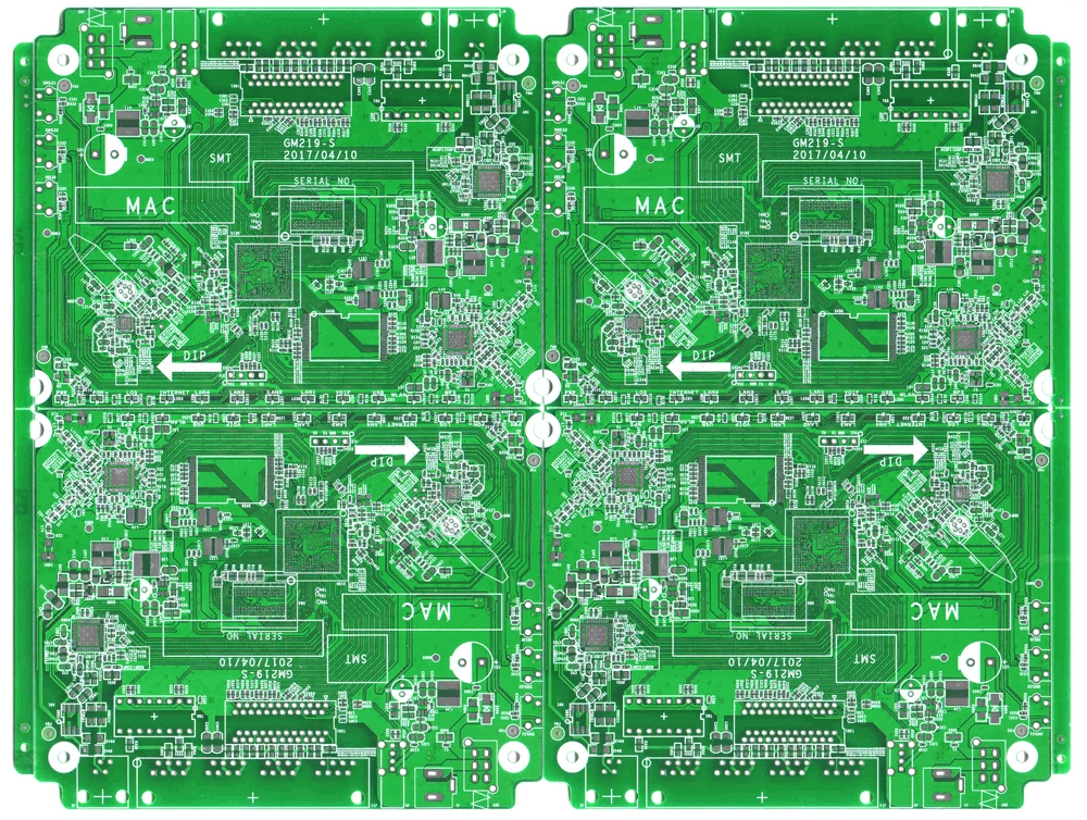
High-frequency PCB — official sample 8 — original catalogue photograph.
High-frequency PCB — official sample 8
Catalogue identification
Sample 8
Material description
High-frequency board; no grade
Published
20 September 2014
Layer count / RF test data
Not specified for this sample
Name the RF laminate grade, design Dk/Df conditions, copper roughness and stack. Request the coupon/test plan at your operating band; the high-frequency label does not establish Rogers, PTFE or a measured loss value.
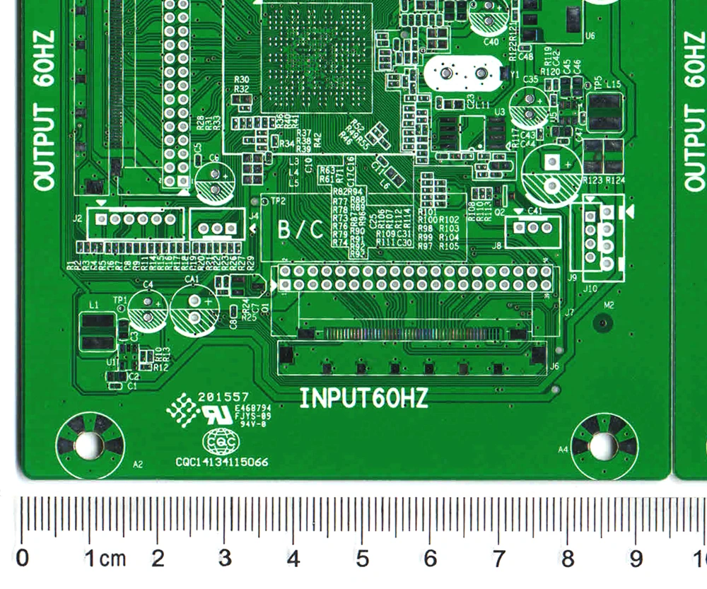
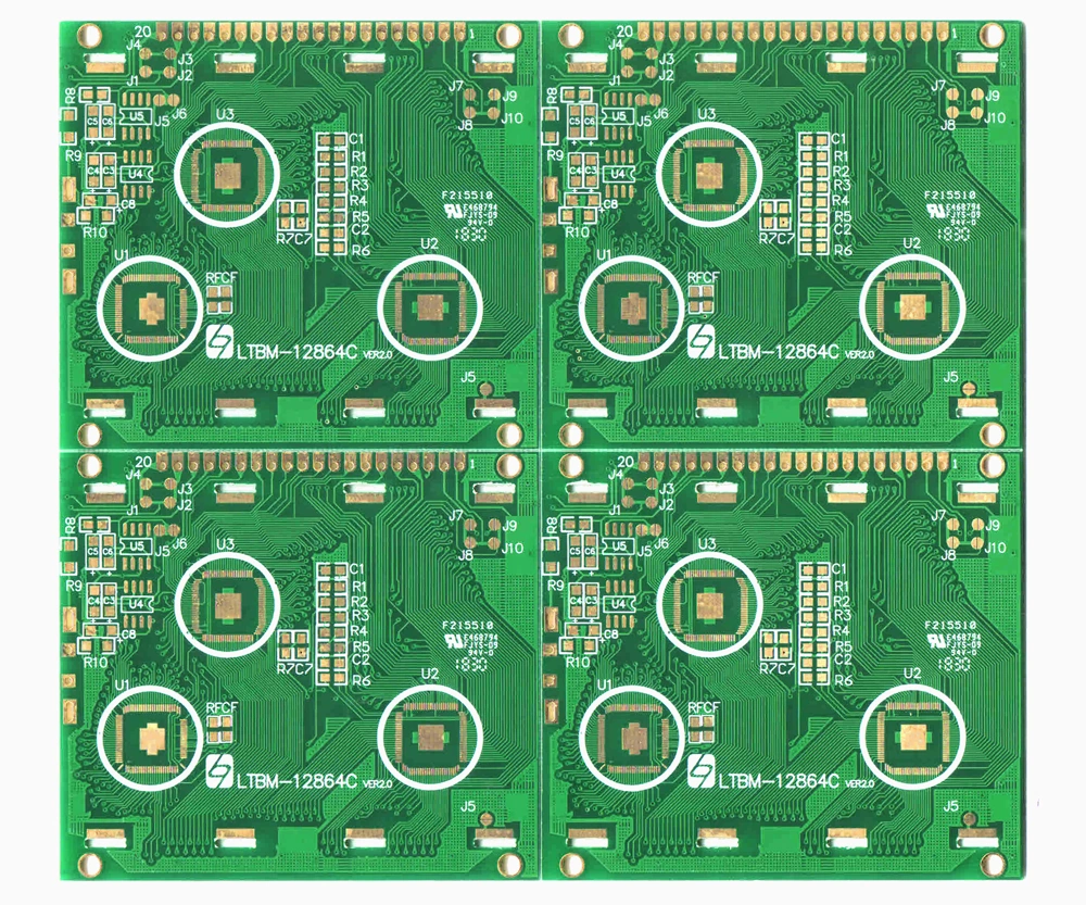
0.10 mm routing PCB — official sample 10 — original catalogue photograph.Second original view on sample 10’s page; no dimensions inferred from the photographed ruler.
0.10 mm routing PCB — official sample 10
Catalogue identification
Sample 10
Line / space stated
0.10 / 0.10 mm; source also calls this 4/4 mil
Published
10 November 2014
Material / layers / finished hole
Not specified for this sample
Confirm 0.10 mm versus exact 4 mil on the controlled drawing, including finished copper and etching allowance. Define pad openings, solder-mask bridge and inspection; do not combine this sample with the six-layer example or general hole limit.
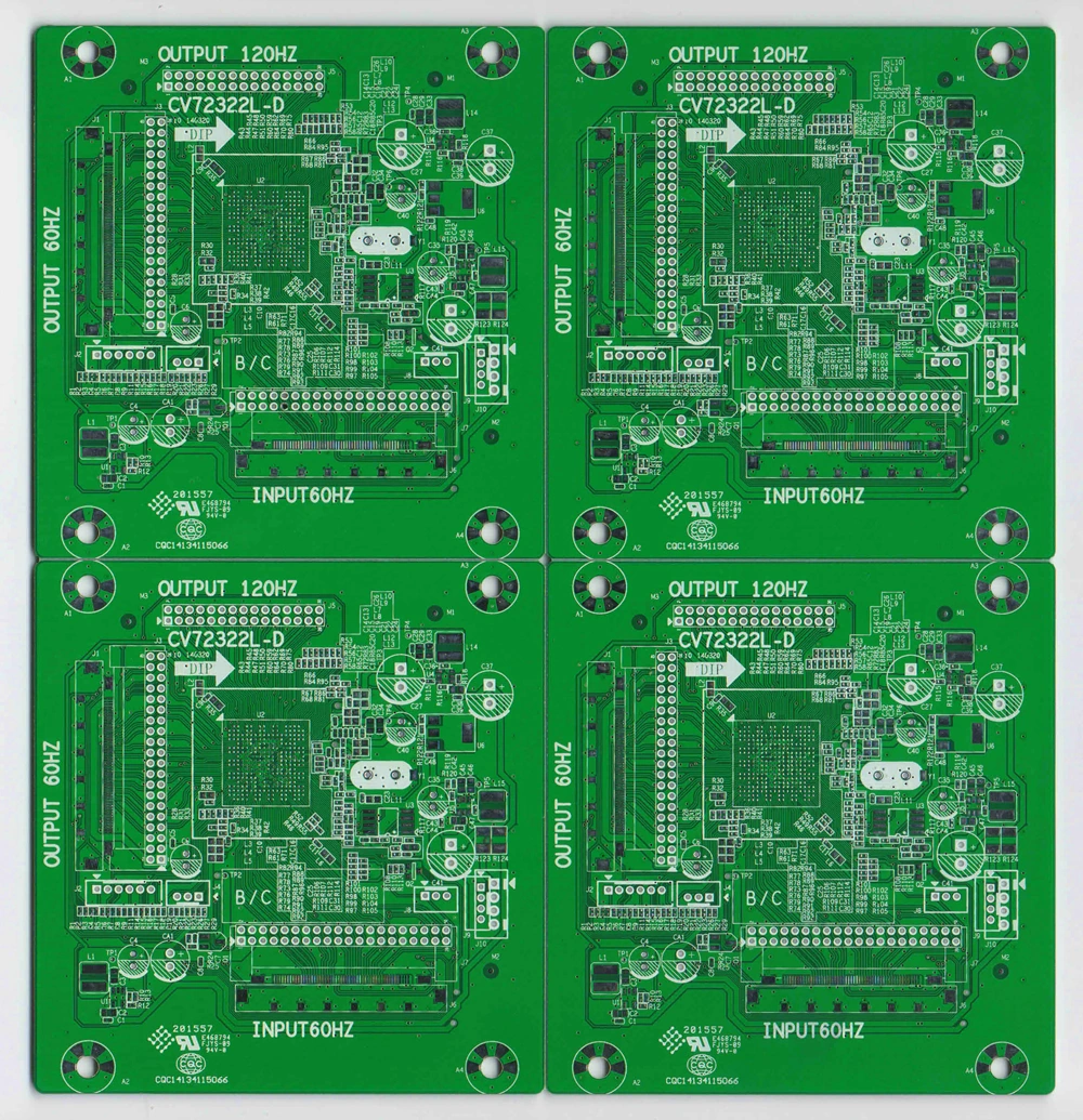
Multilayer PCB — official sample 15 — original catalogue photograph.
Multilayer PCB — official sample 15
Catalogue identification
Sample 15 / multilayer
Published
11 April 2018
Layer count and material
Not specified for this sample
Copper / thickness / finish
Not specified for this sample
Release the actual multilayer stack, laminate grade and finished copper. Define the supplied panel, break-out method and inspection after separation; the photograph is not a panel drawing.
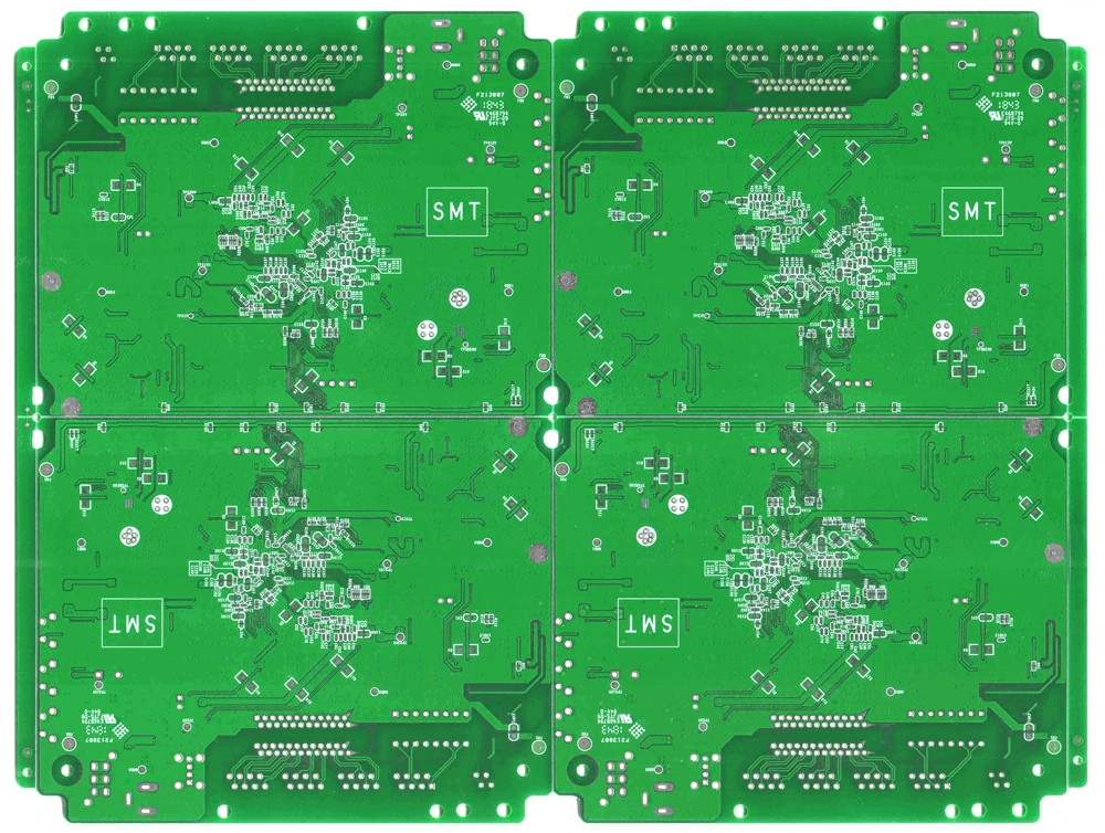
Additional two-sided views: samples 16 and 18
These pages provide corresponding original views but no individual parameter table. Neither board’s end use, layer count, laminate nor copper thickness is assigned from its appearance.
Sample 16 — first original view, published 15 November 2019.Sample 16 — second original view.Sample 18 — first original view, published 15 November 2019.Sample 18 — second original view.
FABRICATION RULES / DEFINE THE FINISHED FEATURE
Check the layer-dependent thickness and hole definitions first.
The official technical page is a general manufacturing table. It does not assign these limits to the particular catalogue photographs or specify which extreme combinations have been qualified.
Stack and panel
Double-sided thickness
0.60–3.00 mm
Two–four-layer thickness
0.60–3.00 mm
Six–eight-layer thickness
1.00–3.00 mm
Double-sided processing size
600 × 800 mm
Multilayer processing size
The separate multilayer row is blank; confirm rather than copy the double-sided limit.
Geometry and separation
Minimum line / space
0.10 / 0.10 mm; also labelled 4/4 mil
Hole diameter row
0.20 mm; drill versus finished bore not defined
Board / hole aspect ratio
10:1
Outline tolerance
±0.10 mm
Hole tolerances
Plated ±0.05 mm; non-plated ±0.10 mm
Line to edge
Routing 0.20 mm; V-cut 0.40 mm
Two details that change the manufacturing instruction
The 0.20 mm hole is not automatically a 0.20 mm finished plated bore. The table groups it under an ambiguously titled hole-distance section and says “diameter.” Request the drill tool, finished bore and copper allowance. No catalogue sample receives this number in its finished-hole filter.
4 mil is 0.1016 mm, not exactly 0.10 mm. The source uses them as parallel labels. Keep the unit, rounding and acceptance on the actual drawing; do not let two differently rounded specifications define inspection.
The same page gives minimum hole copper of 20 µm, solder-mask opening clearance of 0.075 mm and a 0.15 mm solder-mask bridge. It lists FR-4 and aluminium-base material families but no grade-specific process table. Surface treatment is described by customer requirements and RoHS wording, not an explicit finish list. Specify the finish chemistry and thickness yourself.
PROCESS PHOTOGRAPHS / AGREE WHAT IS TESTED
Follow the board from drilling to electrical inspection.
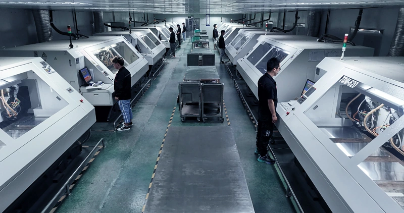
The equipment gallery also shows routing, a vertical continuous pattern-plating line, cleaning, developing, hole inspection, LED exposure, V-cutting and laser marking. These are manufacturer-labelled process photographs; installed quantities, current utilisation and machine-specific qualified tolerances are not established by a gallery.
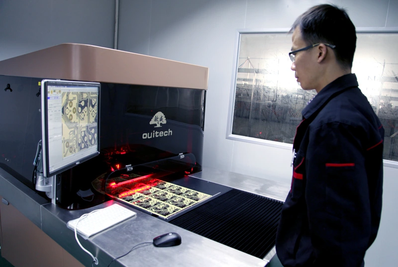
Before image inspection
Agree inner/outer AOI coverage, reference revision, defect classification and repair disposition. A photograph of AOI equipment does not specify what evidence will accompany your lot.
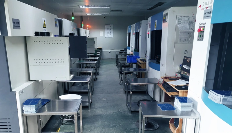
Before electrical release
Specify the released netlist, continuity/isolation requirements and test report. Decide whether flying probe or a fixture is appropriate for the lot, and require traceability between board, panel and report.
Before a compliance claim
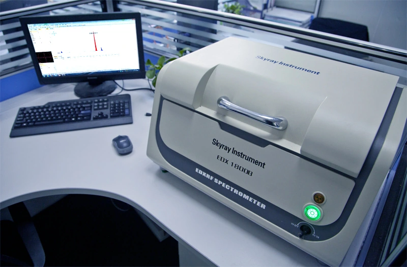
Define the material declaration and any chemical analysis needed for your product. A spectrometer image is not a complete RoHS/REACH assessment of every homogeneous material in an assembled product.
The laser gallery entry is a marking machine, not evidence of laser microvia drilling. The exposure entry is labelled LED exposure, not proof of an LDI process. The official table provides no impedance tolerance; ask for the stack, target, coupon and test method on controlled-impedance work.
WENDU / BUSINESS HISTORY AND SITE RESPONSIBILITY
Use the producing address, not a general brand-history date.
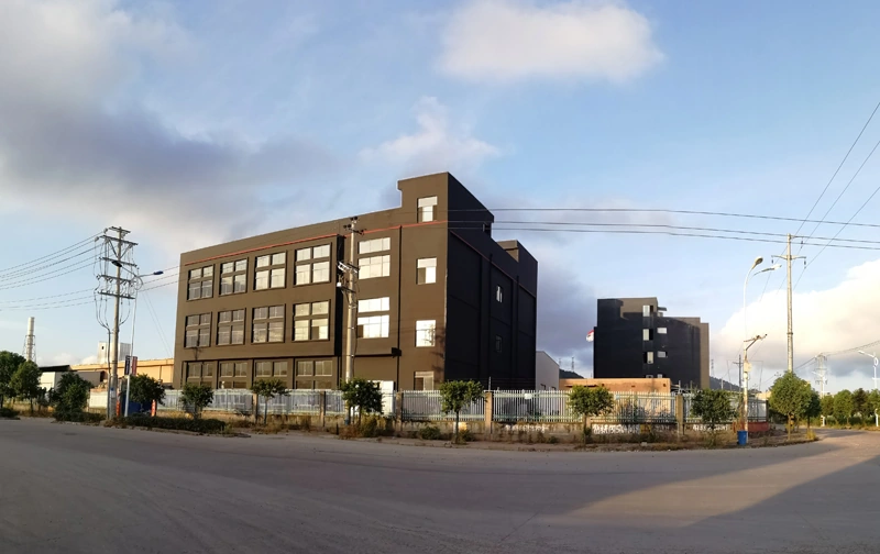
Factory photograph on the manufacturer’s 22 July 2019 phase-two history page.
The official contact page gives No. 11 Yinchuan Road, Wendu Industrial Area, Fuding, Fujian, telephone +86 593 7361299. It publishes fjyspcb@fjyspcb.com and huangxs@fjyspcb.com; these are listed addresses, not proof of mailbox control.
The introduction dates the business history to 2001. Its chronology separately says the Fujian entity registered on 29 July 2013, with groundbreaking that month. Trial production is dated 11 April 2014 in the chronology, whereas the introduction says May 2014. Those differing descriptions are not collapsed into a single verified incorporation or production date.
The 2019 phase-two history entry calls the event an acceptance, while a contemporaneous news headline describes the main building’s construction completion. Neither statement identifies current installed capacity or qualifies every PCB process. Ask which line and site will build the proposed order and approve any subcontracted steps.
Fujian’s original 2025 mandatory cleaner-production audit list, document 闽环保科财〔2025〕20号, includes the exact company at row 513 in Ningde, classified as electronic-circuit-board manufacturing. This corroborates the entity and industry context. Being listed for a required audit is not evidence that the audit was passed or that product quality was approved.
QUALIFICATION / HOLDER, CONSTRUCTION AND DATE
The website’s document copies have specific historical limits.
Management systems
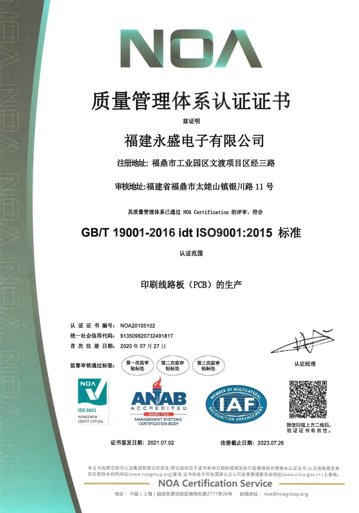
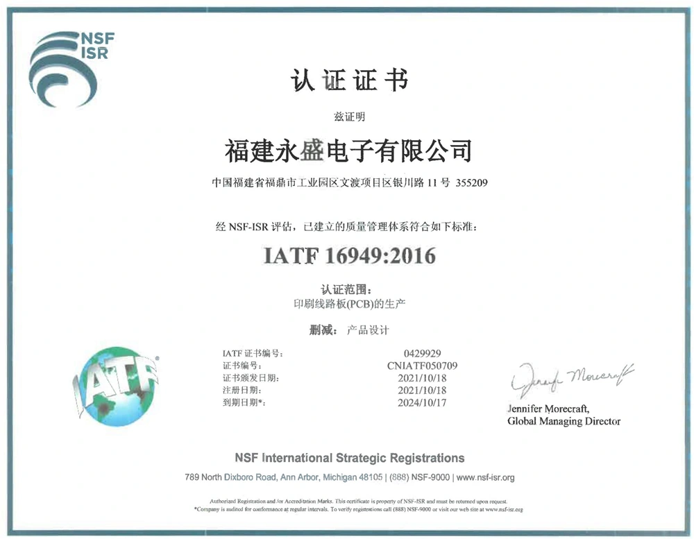
The NOA ISO 9001 copy NOA20105102 covers PCB production and expired 26 July 2023. The NSF-ISR IATF 16949 copy 0429929 / CNIATF050709 covers PCB production, excluding product design, and expired 17 October 2024. The menu’s older “TS16949” label does not change the standard or dates on the actual image.
UL construction
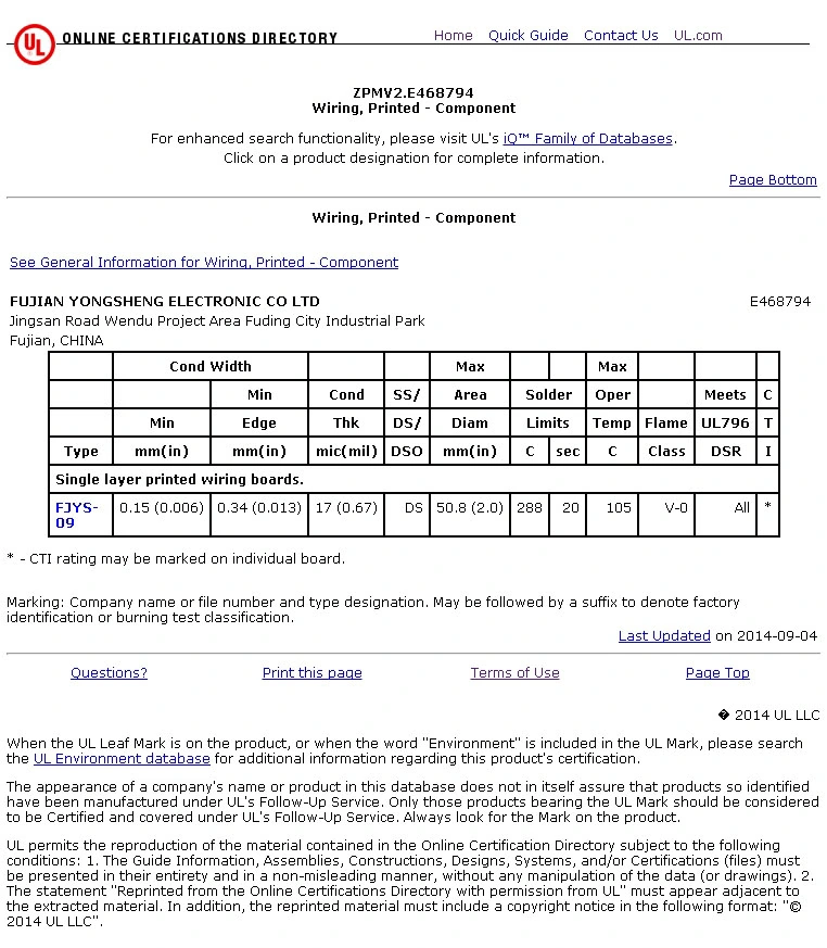
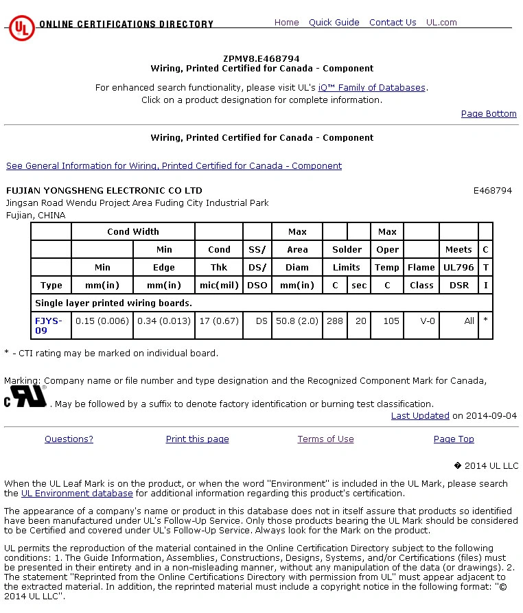
The manufacturer-hosted ZPMV2 and Canada ZPMV8 copies identify FUJIAN YONGSHENG ELECTRONIC CO LTD, E468794, last updated 4 September 2014. The displayed type FIYS-09 is under single-layer printed wiring boards. This dated copy does not certify all multilayer or RF samples, and is not a current independent file-ownership check.
CQC product scope
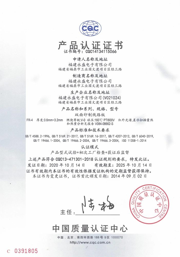
CQC14134115066 names double-sided FR-4 boards, 0.6–3.2 mm, with an expiry of 14 October 2025. That certificate’s range is different from the general factory table; it is neither a current badge nor a reason to widen the table’s 3.0 mm upper thickness.
Read the historical certificate and test-report copies
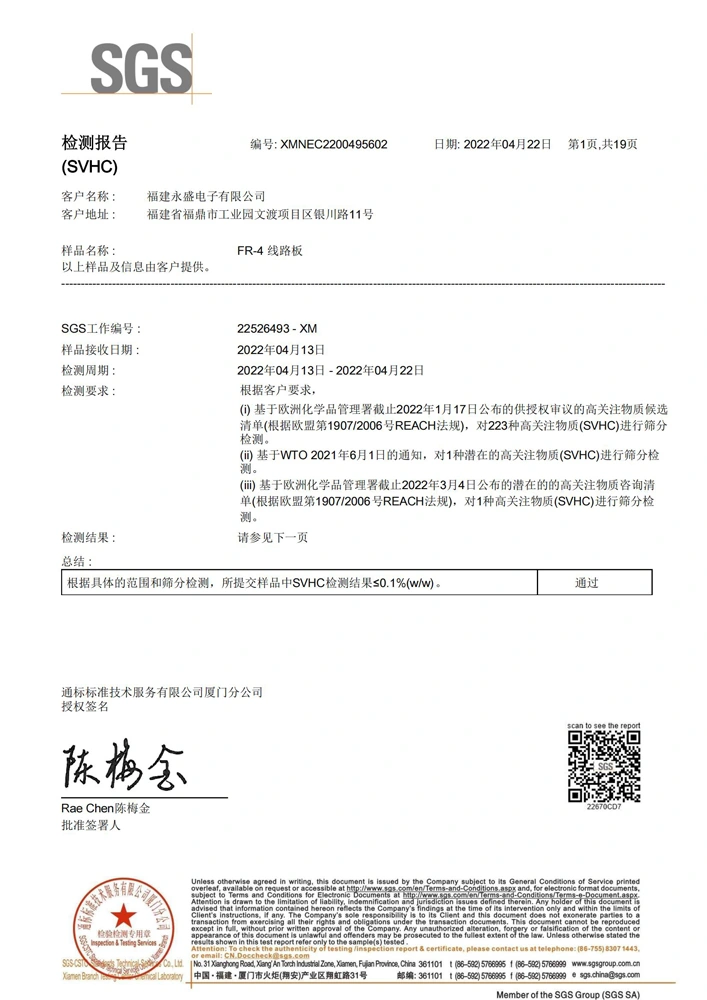
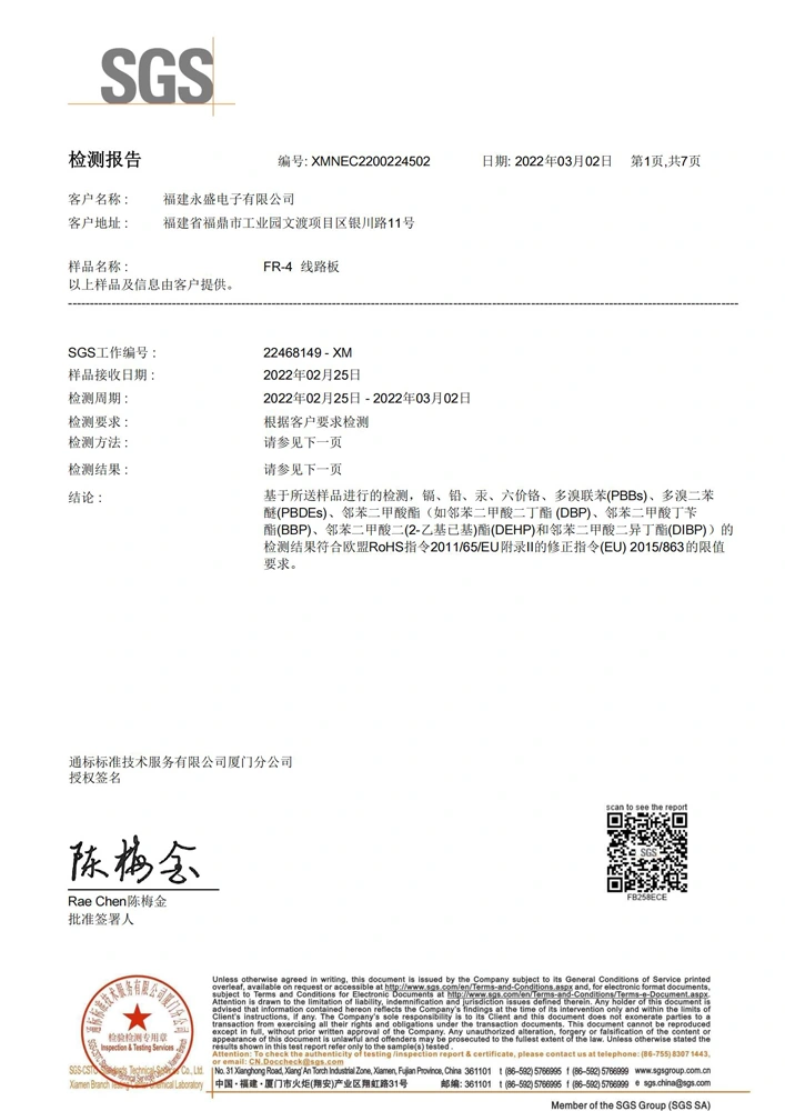
NOA ISO 9001 copy — expiry 26 July 2023.NSF-ISR IATF copy — expiry 17 October 2024.ZPMV2.E468794 — dated 4 September 2014; FIYS-09 single-layer scope.Canada ZPMV8.E468794 — same dated single-layer scope.CQC14134115066 — double-sided FR-4; expiry 14 October 2025.SGS XMNEC2200495602, 22 April 2022 — first of 19 pages, submitted FR-4 SVHC sample.SGS XMNEC220024502, 2 March 2022 — first of seven pages, submitted FR-4 RoHS sample.
The hosted SGS first pages concern submitted FR-4 samples: the April 2022 SVHC report refers to 223 candidate substances plus two additional entries, while the March 2022 report concerns listed RoHS substances. They do not establish every current lot, the current candidate list or the compliance of a complete assembly. Request the applicable current holder/site records and order-specific material traceability before using certification on your own product.
DRAWING RELEASE / GET A COMPARABLE QUOTATION
Close the gap between a numbered sample and your board.
Identify the reference: sample 7, 8, 10 or 15, plus your revision-controlled fabrication package. Keep its disclosed fact separate from your new design.
Define the construction: layer stack, material grade, finished copper and thickness; RF material conditions and impedance coupons where needed.
Define holes and separation: drill versus finished bore, plating, annular rings, routed/V-cut edge clearances and delivered panel.
Define inspection: AOI, netlist test, dimensional and material records, sampling and nonconformance disposition.
Define the supplier scope: Wendu producing line, legal contracting party, applicable current qualifications and any separately quoted SMT/test work.
Reviewed 9 October 2026 against individual sample, equipment, document and history pages, original images and the original Fujian government list. Historical examples do not become combined processing guarantees.
SOURCE TRAIL
Sources behind this profile
Individually reviewed 9 October 2026. Original sample parameters, general manufacturing rules, equipment photographs and dated document copies have different scopes. The independent government list records a required audit, not its completion or product approval.