


Fine bonding pads and finish zones come before a general line-width target.
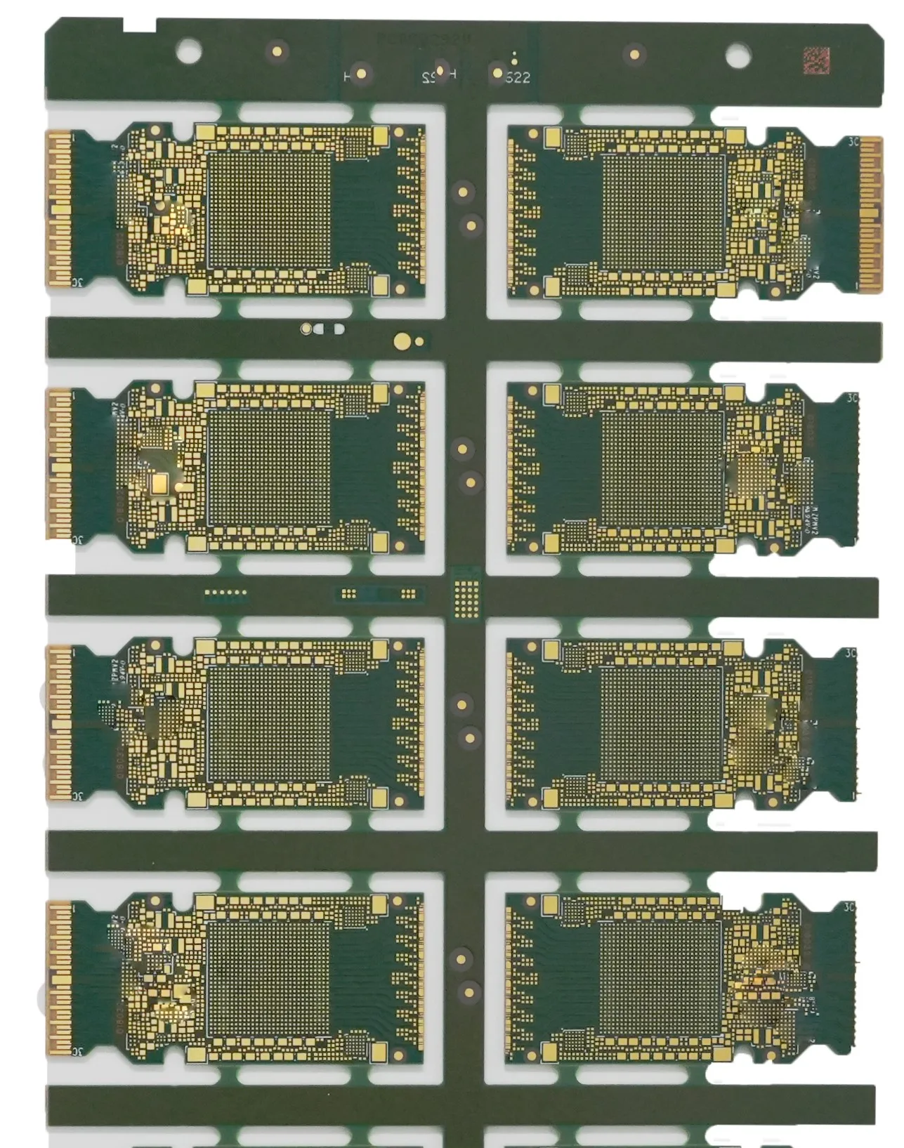
- Construction
- 12-layer HDI · 4+4+4
- Material
- TU883-SP
- Thickness / array
- 1.0 mm · 101 × 260 mm
- Line / space
- 2.5 / 2.5 mil
- Impedance tolerance
- ±7%
- Finish
- ENEPIG + G/F
- Bonding-pad pitch
- 0.13 mm
These values describe this catalogue construction. The 0.13 mm figure is pad pitch, not pad width or a finished-hole diameter. The array dimension is also different from the finished outline of one module. Supply both drawings so the fabricator can assess handling rails, registration and separation without deriving dimensions from the photograph.
Annotate the bonding and connector zones.
The source lists ENEPIG and G/F together without assigning the finishes to individual features or giving deposit thicknesses. Mark those zones in the fabrication drawing, define the required finish and thickness at each interface, and identify the downstream bonding or connection process. Agree the measurement and acceptance record for the fine-pitch pads before releasing the panel.
For the ±7% impedance requirement, state the target impedance, layer and geometry, reference planes, coupon design and measurement method. Ask which stack revision and material lot the fabricator will use. An application label of “800G” does not itself specify a lane rate, channel-loss budget or completed link-test result.
Write the hole table before accepting the back-drill plan.
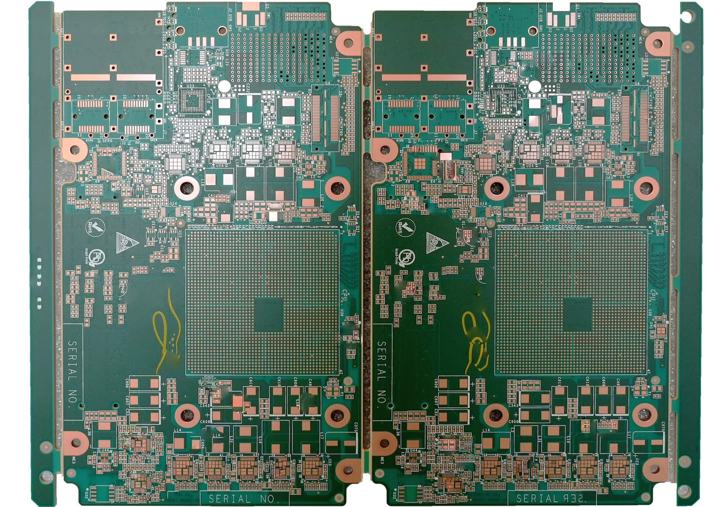
- Layers / material
- 18 layers · M4S
- Thickness / array
- 2.52 mm · 167 × 211 mm
- Drill bit / aspect ratio
- 0.25 mm · 10:1
- Line / space
- 3.0 / 3.0 mil
- Finish
- OSP
- Named processes
- Back-drill · HDI · skip-via · POFV
The source explicitly calls 0.25 mm the minimum drill bit. Keep the plated finished-hole diameter and its tolerance in separate drawing fields. The catalogue’s 10:1 ratio is not a maximum for all Founder boards, and the optical example’s ±7% impedance tolerance should not be copied into this entry, which supplies no impedance tolerance.
Back-drill definition
List the affected nets, drilling side, target stop layer, maximum residual stub and keep-out clearance. Ask how depth and registration are controlled and what coupon or section will be returned. “Back-drill included” is insufficient when the high-speed channel depends on a particular remaining stub.
Via construction
Identify each HDI, skip-via and POFV location on the stack and hole drawings. Obtain the proposed fill, planarization and cap acceptance where applicable, plus the microvia reliability test scope. Do not assume that every hole in the photographed panel uses every named process.
Define the required M4S grade, dielectric construction and permitted substitutions. For OSP, agree storage, packaging, assembly timing and any process-specific handling requirements with the receiving assembler. The source does not publish a shelf-life or an allowable number of reflow cycles for this board.
Ask for one coordinated response from the named plant.
- Freeze the board revision.
Send the finished outline and panel drawing, netlist, layer stack, copper and dielectric definitions. For the optical design, include bonding-pad geometry and finish zones; for the NIC, include the drill/finished-hole table and back-drill schedule.
- Request an annotated feasibility response.
Have the fabricator mark accepted and revised dimensions on that revision. Confirm which features can run together, which are sample-only, and the producing site for the quoted quantity. Any departure from material or stack requirements needs approval before tooling.
- Agree the release evidence.
Specify impedance coupons and the measurement plan where required, relevant sections and hole/deposit measurements, electrical-test coverage, lot identification and the inspection report. Keep the first-article acceptance tied to the process and site proposed for repeat production.
If the sample is assigned to QTA F5 and volume to F3 or another group plant, ask for a transfer qualification plan and the production stack revision. A common legal entity does not make two process routes interchangeable. The procurement response should identify any subcontracted step and who controls the acceptance record.
Prepare the fabrication brief → · Compare HDI constructions →Which records belong to F3, and which belong to the group?
The plant map and the legal entity
The manufacturer map locates F3 at Qianwu Founder Science Park and lists 48,000 m² of plant area and 400,000 ft²/month of productivity. It gives no date for those figures; they are map disclosures, not available capacity reserved for a buyer. F5 is separately listed as QTA, while Chongqing F6 and Zhuhai multilayer F7 have their own entries. Their capacities should not be added to an F3 quote.
The parent issuer’s 2025 annual report identifies 珠海方正科技高密电子有限公司 as a subsidiary producing and selling printed circuit boards. The January 2026 equipment tender published on the Ministry of Commerce platform names the same legal entity at 3209 North Zhufeng Avenue, Doumen. Use the complete address and plant designation in the purchase and quality documents; the group website’s general industrial-base footer is not a site allocation for your board.
Equipment procurement is a dated event
The 29 January 2026 notice is a second tender for a six-axis CCD depth-controlled routing/forming machine, project 0730-264012SZ0014/01. It establishes a procurement notice, not delivery, installation or a measured process tolerance. If your design needs a routed recess or controlled-depth feature, ask for the current machine/process assignment, drawing tolerance and inspection method. No laser-drill model or quantity is inferred from the exterior photograph or this routing tender.
Current group development has a separate scope
The 2025 report describes group batch deliveries for 800G/1.6T optical modules and ≥40-layer production, while describing FVS as small-batch capability. These are issuer disclosures about the group; they do not replace an F3-specific process response. Its Zhuhai AI/compute HDI investment involves both the high-density and multilayer subsidiaries.
The report also describes the Thailand project as entering capacity ramp-up during the reporting period. This is newer than the manufacturer company page’s “under construction” wording. Neither description establishes which site will build the two catalogue examples or the current availability of a particular line.
A recorded standards contribution
The national standards platform lists this exact entity among the drafting organizations for GB/T 46892-2025, the thermal-conductivity test method for electronic circuit boards for high-brightness LEDs, effective 1 July 2026. It is a contribution to a defined test-method standard, not an optical-module qualification, product certification or thermal measurement of either board shown here.
The IFOUND R&D page describes its research organization, patents and historical standards work, with several figures explicitly dated to 2022. Research history can inform supplier discussions, but the order should be released against the current producing-site process window and agreed tests.
Sources behind this profile
Individually researched on 8 October 2026. Group catalogue examples, the named F3 site, issuer disclosures and procurement events retain their distinct scopes. The header uses the official IFOUND group mark; the manufacturer site’s small logo files returned blank colour strips.
- MANUFACTURER / F3 SITENamed F3 HDI and separate F5/F6/F7 entries, with the corresponding F3 photograph ↗
- MANUFACTURER / OPTICAL MODULE800G catalogue image and construction-specific parameters ↗
- MANUFACTURER / SMART NIC18-layer catalogue example; drill-bit and process definitions ↗
- MANUFACTURER / COMPANYGroup locations and dated company background ↗
- MANUFACTURER / R&DResearch institute and historically dated patent/standards statements ↗
- ISSUER / 2025 REPORTOriginal annual report: p5 identity, p11–12 technology, p19 investment, p22 subsidiary ↗
- MOFCOM PLATFORM / TENDER29 January 2026 procurement notice: entity, address and depth-controlled routing machine ↗
- NATIONAL STANDARDS PLATFORMGB/T 46892-2025: test-method title, drafting entity and effective date ↗
- ISSUER / BRANDIFOUND group mark from the parent issuer’s official report index ↗