Mechanical connection
Press-fit holes, insertion and board support.


MANUFACTURER DOSSIER
江苏迪飞达电子有限公司 · Jiangsu
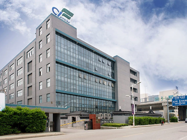
Jiangsu Difeida Electronics — 江苏迪飞达电子有限公司 — places its business in Huangqiao, Xiangcheng District, Suzhou. Its company account dates the business to March 1997. The official catalogue goes beyond a single multilayer range: it shows press-fit connections, server boards, RO3003/FR-4 mixed lamination, PTFE HDI, embedded copper and aluminium-base constructions.
These routes solve different engineering problems. A press-fit order starts with the connector and plated-hole fit; an RF order starts with the material stack and electrical test; a thermal order starts with the heat-transfer and insulation interfaces. Select the relevant example below, then give the factory your released drawing and acceptance requirements.
The company also names FPC, rigid-flex and IC substrates in its introduction. That broader statement does not supply a qualified stack or process window for your design. The examples here retain only their individually published facts.
Press-fit holes, insertion and board support.
Mixed laminates, HDI build-up and channel tests.
Embedded copper, dielectric and contact surfaces.
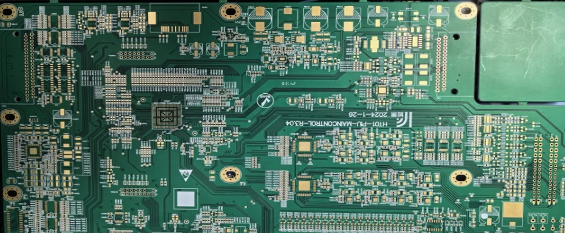
The product title establishes 12 layers and a press-fit connection feature. It does not state the finished hole diameter, plating thickness, connector pin specification or insertion-force window.
Send the connector drawing and the hole map. Agree the finished plated-hole limits, hole-wall copper and acceptance method with the connector requirement, rather than using a generic PCB drill minimum. Identify supported areas during insertion, allowable board deformation and the inspection or extraction tests required for the assembled connection.
The manufacturer's general PTH tolerance is not automatically tight enough for your particular press-fit contact. Ask for a drawing-specific feasibility answer and sample qualification before releasing a production lot.
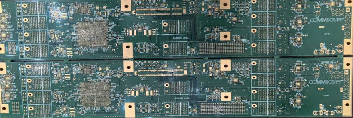
This is a separate 24-layer example. The title does not publish a laminate grade, board thickness, channel rate, back-drill design or loss result. The process table also lists 24 as its multilayer maximum; neither fact supplies your complete server stack.
Release the material grades and layer order, reference planes, differential geometries, via stubs and test coupons. Where back-drilling is required, define the reference surface, remaining stub and keep-out, and request the relevant sectioning or depth-control record. Agree the electrical acceptance your channel needs, rather than treating a server application label as a bandwidth rating.
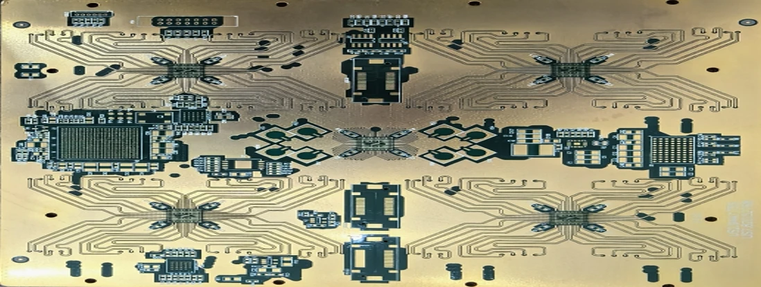
The named construction is 18 layers, RO3003 and FR-4. RO3003 is an identified laminate; FR-4 remains a family label. The catalogue does not identify the FR-4 grade, material positions, bonding films or finished copper.
Request the layer-by-layer stack and exact dielectric thicknesses. State the RF frequency range, controlled geometry and test method your circuit requires. Agree compatible processing and dimensional tolerances across the mixed materials, and how the delivered lot identifies the approved laminate and any substitutions.
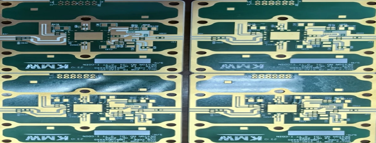
The product is labelled second-order HDI and PTFE. The total layer count and specific PTFE laminate grade are not given. Second-order is a build-up description, not a two-layer PCB.
Supply the via construction, dielectric sequence, capture pads, fill/cap requirements and approved material. Ask the laser-drilling division to review the actual laminate/via combination and agree microvia inspection and reliability tests. Do not transfer the other example's 18 layers or RO3003 grade into this PTFE entry.
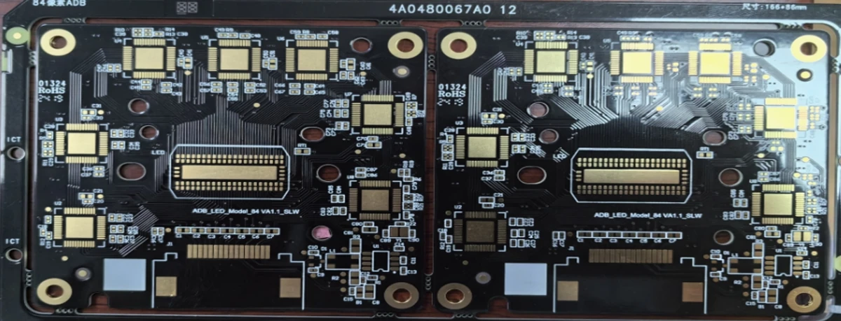
The catalogue identifies four layers and an embedded copper block, intended for heat dissipation. It supplies no thermal resistance, block dimensions, surface-height tolerance or measured temperature rise.
Show the copper block and component contact on the mechanical section. Define insulation clearances, flushness or protrusion, attachment and thermal interface. Agree how block position and interfaces are inspected. A copper-block photograph cannot establish the temperature your assembled product will achieve.
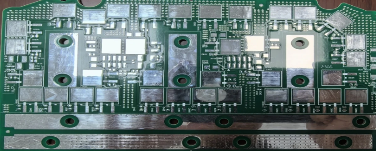
The original Chinese label is “双侧双面铝基板4oz”. It names an aluminium-base construction and 4 oz copper, but does not resolve the complete metal/dielectric layer arrangement or whether that copper figure is starting foil or finished copper.
Provide a section drawing and confirm which circuit layers the copper figure covers. Specify the dielectric grade, thickness, insulation test and thermal requirement, plus any holes that must remain isolated from the metal base. Treat the published aluminium-board process rules as a feasibility starting point, not an acceptance certificate.
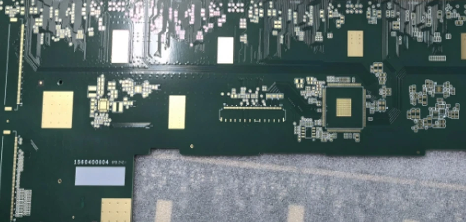
The product title supplies six layers and 0.6 mm thickness. The laminate, trace/space, contact finish and electrical test are not specified for this example.
Release the thickness tolerance, outline and connector datum, supported areas and component or fixture clearances. Agree panelisation, depanelisation and handling through assembly so the delivered geometry can be inspected against your drawing. Define any optical-module electrical or contact requirements separately; the application name alone does not give a data-rate or optical-performance rating.
The website publishes separate double-sided, multilayer, HDI and aluminium-board tables. These are manufacturer-stated process envelopes. The following selected entries are useful for engineering review; they are not assigned to the seven photographed products above.
The 0.1 mm through-hole minimum is not explicitly defined as a finished plated-hole diameter. The table separately gives PTH ±0.075 mm and NPTH ±0.05 mm tolerances. Request the actual finished-hole limits for the selected stack.
The notation H/H and 1/1 or 2/2 belongs to the supplier's copper-conditioned chart. Confirm its copper definition and which rule applies to a 4 oz design. Do not use the smaller figure without that review.
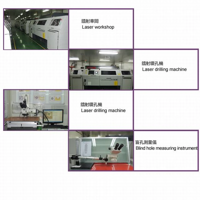
The labelled gallery shows a laser workshop, laser-drilling machines and a blind-hole measuring instrument. It does not identify current machine capacity or calibration. The HDI chart lists ±15 µm laser alignment, ≤15 µm dimple and a 0.75:1 blind-hole aspect ratio. Ask which material and via geometry those limits cover, and request the agreed sectioning or inspection record on your construction.
For press-fit or high-layer orders, define the plating, via fill, back-drill and inspection records required with the shipment. For a repeat order, keep the approved stack, supplier material substitutions and fabrication changes under the same revision control as the board artwork.
The contact page identifies Muxiang Industrial Area, Huangqiao. The readable quality documents use Wangsheng Road 176; the ICAS ISO copies also list a Dazhuang electroplating industrial-park site, Building 5. Establish which legal entity and manufacturing/finishing sites are included in the quotation and inspection plan.
The URS IATF 16949 front page names Jiangsu Difeida, Wangsheng Road 176, IATF number 0497826 and a 25 January 2024–24 January 2027 period; the attachment covers PCB manufacture, excluding product design under clause 8.3. It lists an extended manufacturing site at the ground floor of Building 5, Dazhuang Electroplating Industrial Zone, Dadong Road, with PCB drilling as its stated scope. The NQA IECQ QC 080000 copy covers PCB production and prints expiry 16 May 2027. The ICAS ISO 9001/14001 copies show 17 January 2026–16 January 2029, while ISO 45001 shows 27 April 2025–26 April 2028.
These dates and scopes are read from displayed copies. Check the applicable attachment, current issuer status and site scope for your order; they are not an independent PCBVerified factory audit.
The Suzhou Ecology and Environment Bureau's 16 March 2026 notice identifies Difeida's high-density integrated-circuit R&D and production project. The original approval places it west of Yinliwan Avenue and south of Yongshui Road in Huangqiao and describes planned annual PCB and component-placement capacity.
This is a project environmental approval with construction, pollution-control and completion conditions. It does not prove that the new capacity is operational or that the photographed products are qualified there. Ask which existing or new site will fabricate, plate, assemble and release your order.
Individually researched 8 October 2026. Product titles and original photographs were checked separately from the general process tables. Unpublished product-level line, hole and impedance values remain unknown. Procurement questions are editorial guidance; certificate copies and project approval remain distinct from current independent verification.
We use cookies to provide our services and measure website usage. Privacy policy