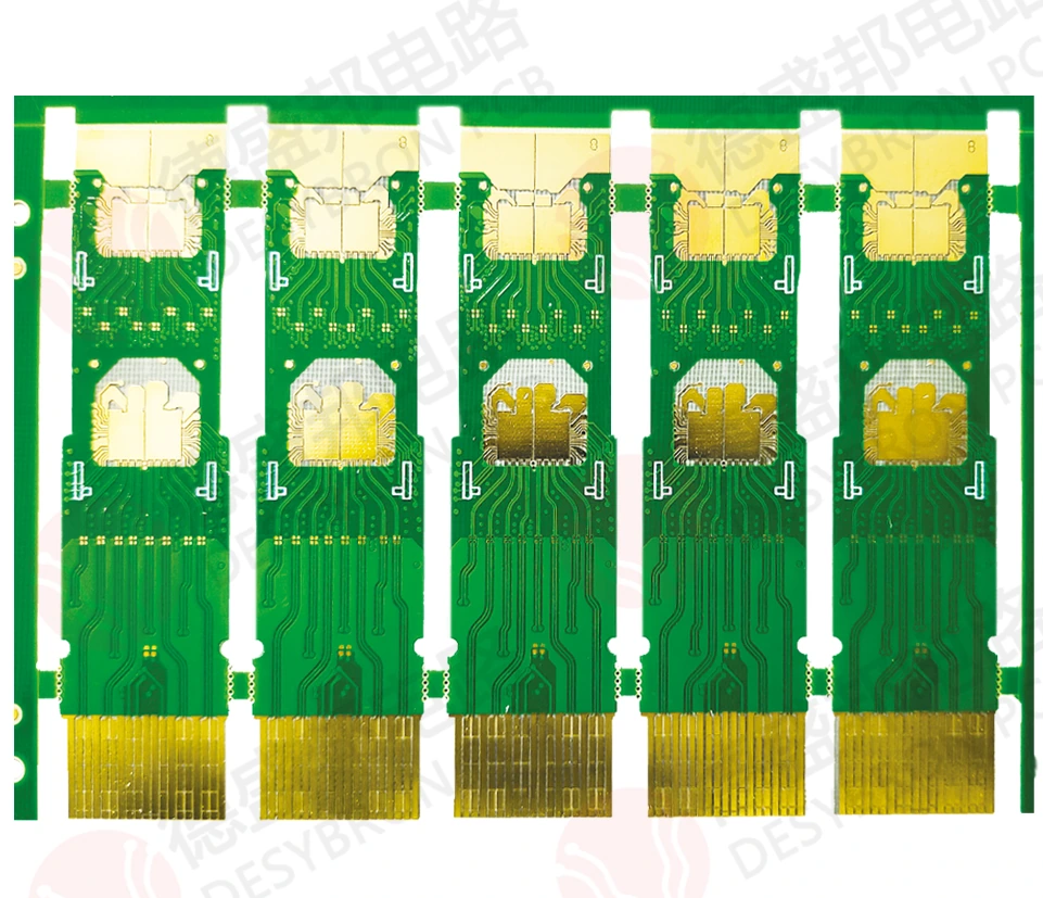
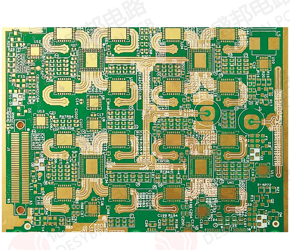
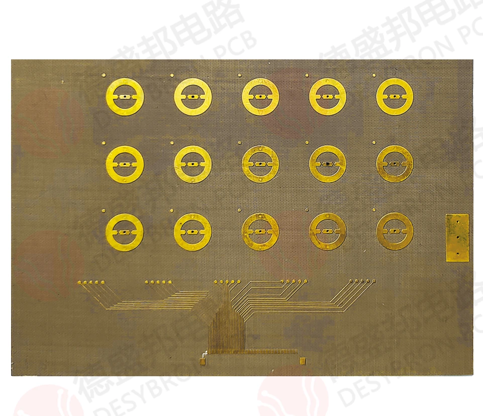
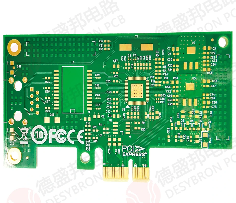
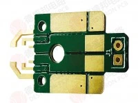
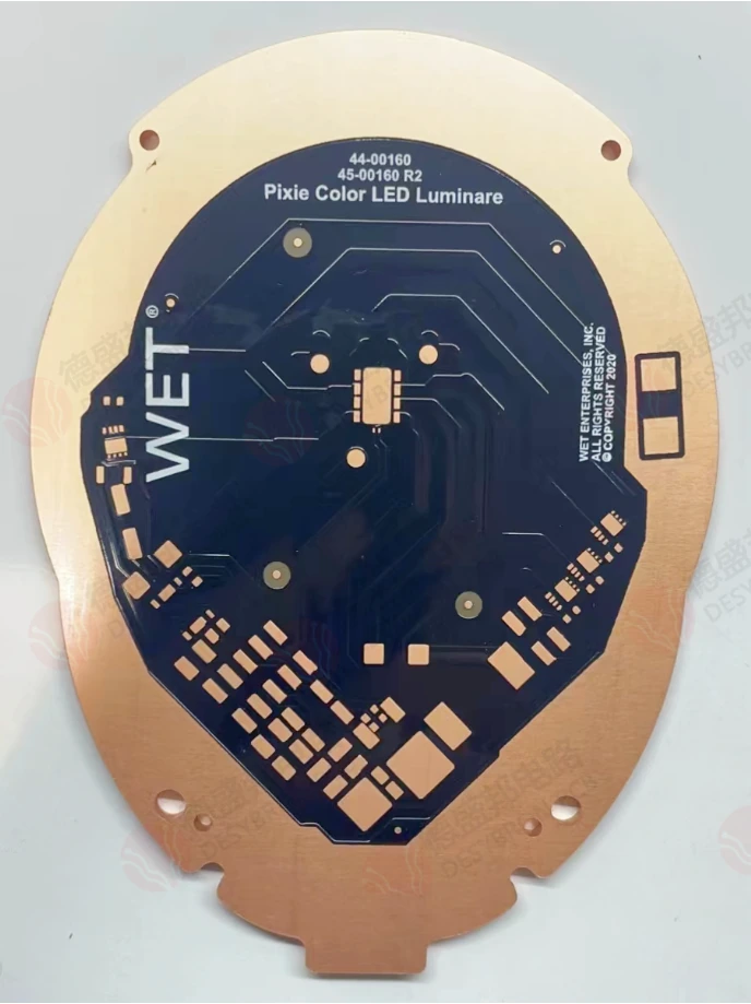
Start with the laminate, contact surface and mechanical interface.
深圳市德盛邦电路技术有限公司 uses SHENZHEN DESYBRON PCB TECHNOLOGY CO., LTD on its official website. The Shenzhen company describes RF and microwave boards, mixed-material multilayers, high-density work and special constructions. Its catalogue is particularly useful where the board is also a mechanical or thermal component: local thick-gold contacts, backdrilled connections, stepped test fixtures, copper-base lighting and thick-copper optical modules.
The examples below preserve their own parameter tables. A material name is a catalogue statement, not evidence of material purchased for your order. Likewise, a “medical” or “aerospace” application label is not programme qualification. Specify the operating conditions and delivered inspection records for the actual design.
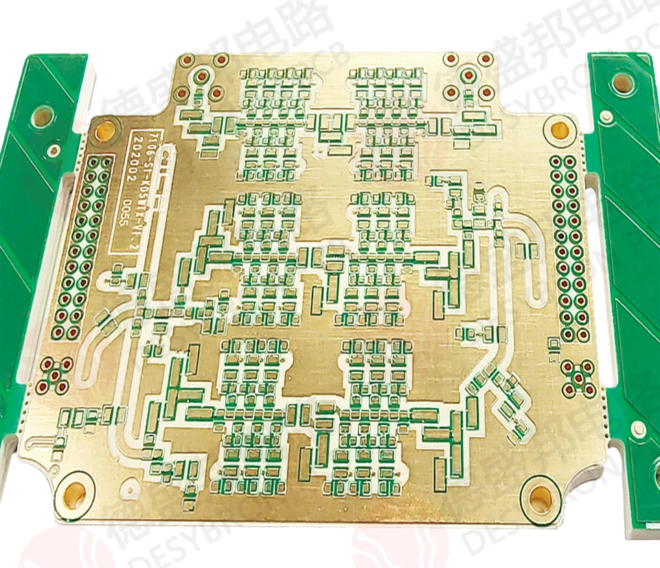
RF / MIXED LAMINATION / LOCAL PLATING
Four communication constructions solve different problems.
A ten-layer count hides important differences. The IT968TC example separates general gold from local thick-gold contacts. The RO4350B example uses ENEPIG. The mixed-lamination example names TU-872SLK and Rogers 4350b together. Keep those differences in the fabrication drawing and quotation rather than comparing the examples by layer count alone.
Individual catalogue construction · manufacturer-published values
Ten-layer IT968TC communication board
Layers
10
Material
ITEQ IT968TC
Thickness
1.0 mm
Copper
1 oz
Contact finish
Gold 2 µin; local thick gold 50 µin
Trace / space
3 / 3 mil
Separate local contact plating from the general gold finish. Release the contact-zone drawing, nickel underplate, bevel and thickness acceptance.
Individual catalogue construction · manufacturer-published values
Ten-layer RO4350B communication PCB
Layers
10
Material
Rogers RO4350B
Thickness
2.2 mm
Copper
1 oz
Finish
ENEPIG
Trace / space
6 / 6 mil
Request the complete dielectric stack and lamination construction: the named laminate does not establish whether all ten layers use the same material. Define ENEPIG thickness and RF coupon acceptance.
Individual catalogue construction · manufacturer-published values
Four-layer RO4003C antenna PCB
Layers
4
Material
Rogers RO4003C
Thickness
1.6 mm
Copper
1 oz
Finish
Immersion gold
Trace / space
3 / 3 mil
Give operating frequency, stack geometry, controlled impedance, via transition and coupon requirements. The catalogue does not supply measured RF loss or a per-product impedance tolerance.
Individual catalogue construction · manufacturer-published values
Ten-layer mixed-laminate RF PCB
Layers
10
Material
TU-872SLK + Rogers 4350b (source notation)
Thickness
1.6 mm
Source minimum hole
0.2 mm; finished-hole definition unstated
Finish
Immersion gold
Trace / space
2.5 / 2.5 mil
Identify the RF and FR-4 layers, bonding materials and lamination cycles. Request registration and thickness controls for the mixed stack rather than applying one material property to every layer.
MODULES / STUBS / STEPS / CONTACT EDGES
Release the three-dimensional drawing with the artwork.
Individual catalogue construction · manufacturer-published values
Ten-layer backdrilled IoT module PCB
Layers
10
Material
Exact grade not published
Material label
Taiwan Union; exact grade not published
Thickness
1.8 mm
Thickness tolerance
Source range 5–7%; interpretation to agree
Finish
Immersion gold
Process
Backdrilling
Specify the backdrill side, diameter, target layer and maximum residual stub. Supply the exact laminate grade, impedance stack and drill-to-copper clearance; a backdrill label alone is not a high-speed validation.
Individual catalogue construction · manufacturer-published values
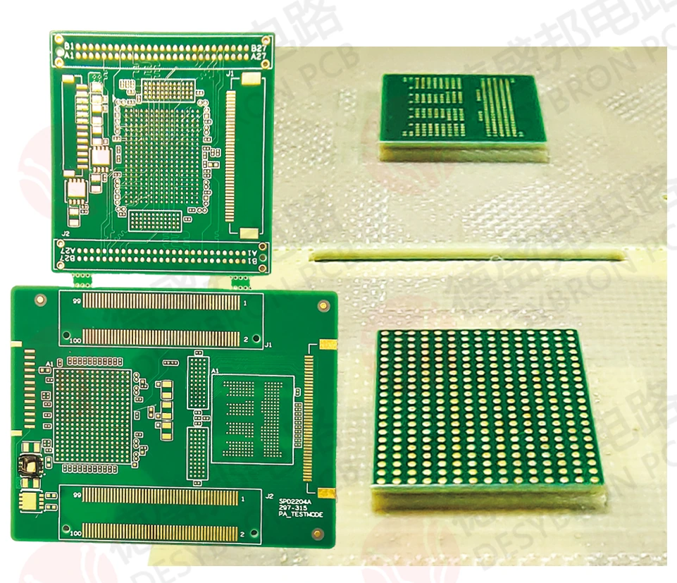
Eighteen-layer semiconductor test PCB
Layers
18
Material
S1000-2M
Thickness
2.8 mm
Thickness tolerance
Source range 5–7%; interpretation to agree
Process
Stepped construction
Finish
Immersion gold
Provide the step drawing, depth datum, probe interface and actual flatness acceptance. The page’s “flatness ≥2” has no units or test definition and is not adopted as a specification.
Individual catalogue construction · manufacturer-published values
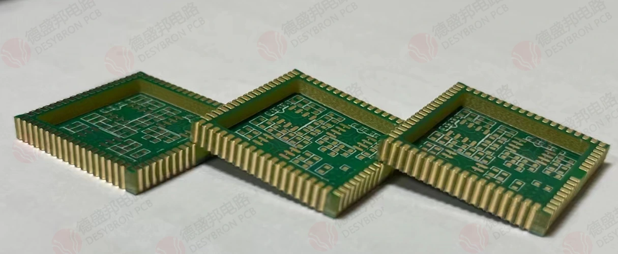
Six-layer half-hole home-control module
Layers
6
Material
Shengyi TG170 (source label)
Thickness
1.2 mm
Copper
1 oz
Finish
Immersion gold
Process
Half holes and source 揭盖 opening process
Trace / space
3 / 3 mil
Release the castellated contact and opening drawings, depth limits and edge-copper acceptance. Confirm the laminate grade and the exact operation meant by 揭盖 before quoting tooling.
Backdrilling
The IoT module page identifies backdrilling but gives no residual-stub limit. Name the entry side and stop layer, drill diameter, remaining stub and inspection evidence. Agree how backdrill clearance is checked against the actual stack.
Stepped test interface
The eighteen-layer test board needs step depth, datum and probe-interface dimensions. Its “flatness ≥2” entry has no units or method, so it is excluded from the specifications. Supply a measurable flatness requirement and fixture support condition.
Castellated module
The six-layer home-control example names half holes and 揭盖. Confirm the specific opening operation and exposed layer, then dimension the contact edge. Ask how plating wrap, burr and depanelisation condition will be inspected.
COPPER / HEAT / ELECTRICAL ISOLATION
Heavy copper and a copper base are different constructions.
The optical and industrial-laser examples specify TG170 with pure copper. The lighting example instead identifies a copper-base substrate. Those descriptions do not supply the same dielectric stack or isolation path; quote them with a section drawing, not just an ounce value.
Individual catalogue construction · manufacturer-published values
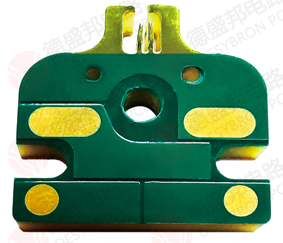
Two-layer thick-copper optical module PCB
Layers
2
Material
TG170 + 0.3 mm pure copper
Thickness
3.4 mm
Copper
0.3 mm; source also labels 8 oz
Gold
Source notation 10U
Contact tolerance
Source ±0.03; units and datum unstated
Release the contact geometry and plating unit, copper measurement basis and thermal interface. Confirm how the 0.3 mm copper value and 8 oz label relate; do not replace them with an assumed conversion.
Individual catalogue construction · manufacturer-published values
Two-layer industrial laser test PCB
Layers
2
Material
TG170 + 0.4 mm pure copper
Thickness
1.0 mm
Top copper
0.4 mm; source also labels 11 oz
Gold
Electroplated gold, source notation 10U
Process
Cut-out contact fingers
Dimension the cut-outs and exposed contacts, define current and temperature rise, and agree plating units. The source’s finger tolerance ±0.03 does not name a unit or datum.
Individual catalogue construction · manufacturer-published values
Two-layer copper-base lighting PCB
Layers
2
Material
Copper-base substrate; grade unspecified
Thickness
2.0 mm
Source minimum hole
0.5 mm; finished-hole definition unstated
Finish
OSP
Process
Copper base and NC drilling
Trace / space
5.5 / 6 mil
Request the dielectric stack, isolation voltage and through-plane thermal resistance. “High thermal conductivity” is not a numerical material rating; specify mounting, flatness and the delivered outline.
PROCESS TABLE / TWO DIFFERENT COMMERCIAL WINDOWS
Prototype limits are not the volume-production range.
The official technical page explicitly splits sample processing from volume production. The following are separate process-table entries, not a guarantee that every maximum can be combined on the same stack.
Sample processing
Layers
1–50
Finished board thickness
0.2–10.0 mm
Finished copper
0.5–12 oz
Minimum trace / space
2.5 / 2.5 mil
Minimum finished hole
0.10 mm
Maximum aspect ratio
25:1
Impedance control
±10%
Volume production
Layers
1–20
Finished board thickness
0.4–6.0 mm
Finished copper
0.5–6 oz
Minimum trace / space
3 / 3 mil
Minimum finished hole
0.15 mm
Maximum aspect ratio
12:1
Impedance control
±10%
Both columns state a maximum manufacturing size of 610 × 1200 mm. This is not the delivered outline of any photographed board. Unlike the technical table’s explicit finished hole, several product pages say only “minimum hole”; those values remain descriptive and are not assigned as finished-hole filter values.
Other catalogue entries and the limits of their descriptions
The three rigid-flex detail pages provide photographs but only a full stop in the product-content field. No layer count, bend radius or stack is assigned from these images. The BT substrate category has no board detail in the reviewed listing.
The automotive-labelled Arlon 880 example lists 1 oz copper and also “thick copper 4 oz” as a special process without specifying its layer or zone. Those figures are not merged. The industrial blind-via page’s “BGA size 0.15 mm” does not define pitch, land or drill size, so it is not converted into a BGA capability.
SHENZHEN / SCHEDULE / INSPECTION HANDOVER
Confirm the producing address and the order-specific process plan.
The contact page gives Building E5, Yanchuan Northern Industrial Park, Yanchuan Community, Yanluo, Songgang, Bao’an, Shenzhen. The company introduction dates the business to August 2016 and describes a Shenzhen production base; this is manufacturer history, not an independently checked incorporation date. The official sales addresses are sales@dsbpcb.com and mkt@dsbpcb.com, with service contact kf@dsbpcb.com. Reading these addresses does not establish mailbox control; no email was sent.
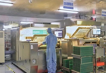
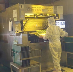
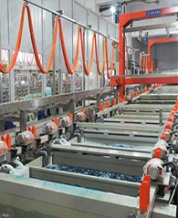
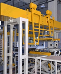
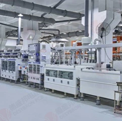
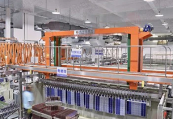
CCD registration · manufacturer-labelled photograph; model and current installed capacity not established.Solder-mask exposure · manufacturer-labelled photograph; model and current installed capacity not established.Automatic copper deposition · manufacturer-labelled photograph; model and current installed capacity not established.Lamination press · manufacturer-labelled photograph; model and current installed capacity not established.Vacuum etching · manufacturer-labelled photograph; model and current installed capacity not established.Automatic electroplating · manufacturer-labelled photograph; model and current installed capacity not established.
The technical page names these production stages but the photographs do not establish machine models, utilisation or which site performs every step. Ask for the process allocation, subcontracted operations, electrical test, coupon/microsection coverage and records included with delivery. No current ISO/IATF copy or UL holder record was identified in the reviewed pages, so no qualification badge is assigned.
Prototype scheduling
The technical page quotes 4 days for two layers, 6 for four, 7 for six, 8 for eight and 8–10 for ten or more. It also advertises a fastest 24-hour expedited service. These are published scheduling statements, not availability for a complex mixed or stepped construction.
Volume scheduling
Small batches are listed at 5–10 days and medium batches at 8–24 days, with staged delivery possible. Confirm quantity, working-day basis, engineering release, laminate availability and inspection time in the quotation.
The first RFQ
Attach the stack and material grades, local-plating map, step/backdrill/thermal drawings, impedance targets and test requirements. Name the contracting and producing entity, site and change-control responsibility. Ask for price and lead time against this package.
Individually read 9 October 2026: company/contact pages, the technical table, 23 product details and their corresponding original images. Product examples and general process ranges are kept separate. An exact corresponding original government or issuer record has not been obtained; no independent site or certificate approval is claimed.